
 5秒后页面跳转

| 是否无铅: | 含铅 | 是否Rohs认证: | 不符合 |
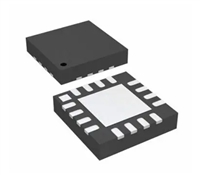
| 生命周期: | Contact Manufacturer | 包装说明: | TBGA, BGA165,11X15,40 |
| Reach Compliance Code: | not_compliant | 风险等级: | 5.58 |
| 最长访问时间: | 8.5 ns | 最大时钟频率 (fCLK): | 87 MHz |
| I/O 类型: | COMMON | JESD-30 代码: | R-PBGA-B165 |
| JESD-609代码: | e0 | 长度: | 15 mm |
| 内存密度: | 4718592 bit | 内存集成电路类型: | CACHE DRAM MODULE |
| 内存宽度: | 18 | 湿度敏感等级: | 3 |
| 功能数量: | 1 | 端子数量: | 165 |
| 字数: | 262144 words | 字数代码: | 256000 |
| 工作模式: | SYNCHRONOUS | 最高工作温度: | 70 °C |
| 最低工作温度: | 组织: | 256KX18 | |
| 输出特性: | 3-STATE | 封装主体材料: | PLASTIC/EPOXY |
| 封装代码: | TBGA | 封装等效代码: | BGA165,11X15,40 |
| 封装形状: | RECTANGULAR | 封装形式: | GRID ARRAY, THIN PROFILE |
| 并行/串行: | PARALLEL | 峰值回流温度(摄氏度): | 225 |
| 电源: | 2.5,3.3 V | 认证状态: | Not Qualified |
| 座面最大高度: | 1.2 mm | 最大待机电流: | 0.03 A |
| 最小待机电流: | 3.14 V | 子类别: | SRAMs |
| 最大压摆率: | 0.18 mA | 最大供电电压 (Vsup): | 3.465 V |
| 最小供电电压 (Vsup): | 3.135 V | 标称供电电压 (Vsup): | 3.3 V |
| 表面贴装: | YES | 技术: | CMOS |
| 温度等级: | COMMERCIAL | 端子面层: | Tin/Lead (Sn63Pb37) |
| 端子形式: | BALL | 端子节距: | 1 mm |
| 端子位置: | BOTTOM | 处于峰值回流温度下的最长时间: | 20 |
| 宽度: | 13 mm | Base Number Matches: | 1 |
| 型号 | 品牌 | 获取价格 | 描述 | 数据表 |
| 71V257985BQI | IDT |
获取价格 |
Standard SRAM, 256KX18, 8.5ns, CMOS, PBGA165 |

|
| 71V257985PF | IDT |
获取价格 |
Standard SRAM, 256KX18, 8.5ns, CMOS, PQFP100 |
|
| 71V30 | RENESAS |
获取价格 |
1K x 8 3.3V Dual-Port RAM |
|
| 71V30L25TFG | IDT |
获取价格 |
HIGH-SPEED 3.3V 1K X 8 DUAL-PORT STATIC RAM |
|
| 71V30L25TFG8 | IDT |
获取价格 |
HIGH-SPEED 3.3V 1K X 8 DUAL-PORT STATIC RAM |
|
| 71V30L25TFGI | IDT |
获取价格 |
Dual-Port SRAM, 1KX8, 25ns, CMOS, PQFP64, 10 X 10 MM, 1.40 MM HEIGHT, GREEN, STQFP-64 |
|
| 71V30L25TFGI8 | IDT |
获取价格 |
HIGH-SPEED 3.3V 1K X 8 DUAL-PORT STATIC RAM |
|
| 71V30L35TF | IDT |
获取价格 |
TQFP-64, Tray |
|
| 71V30L35TF8 | IDT |
获取价格 |
TQFP-64, Reel |
|
| 71V30L35TFG | IDT |
获取价格 |
Dual-Port SRAM, 1KX8, 35ns, CMOS, PQFP64, 10 X 10 MM, 1.40 MM HEIGHT, GREEN, STQFP-64 |
|
 RF5110数据手册详解:3V GSM射频功率放大器的深度分析

 REF1004-1.2手册详解:引脚信息、产品描述、参数分析
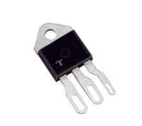 晶闸管的静态特性与伏安特性详解
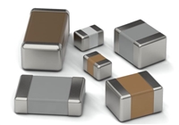 贴片电容的工作原理与参数识别
工作时间:9:00-21:00
CEO邮箱:ceo@jiepei.com
投诉邮箱:tousu@jiepei.com


 浙公网安备 33010502006866号 浙ICP备10014259号-119
营业执照ICP证
浙公网安备 33010502006866号 浙ICP备10014259号-119
营业执照ICP证


