FLASH
AS8FLC2M32
A system reset would then also reset the FLASH device,
enabling the system microprocessor to read the boot-up
firmware from the FLASH memory array. The device offers two
power-saving features. When addresses have been stable for a
specified amount of time, the device enters the AUTOMATIC
SLEEP MODE. The system can also place the device into the
STANDBY mode. Power consumption is greatly reduced in
both these modes.
the power transition. No command is necessary in this mode to
obtain array data. Standard microprocessor read cycles that
assert valid data on the device address inputs produce valid
data on the data outputs. The device remains enabled for read
access until the command register contents are altered.
See READING ARRAY DATA for more information. Refer
to AC Read Operations table data for timing specifications
relevant to this operational mode.
Device Bus Operations
This section describes the use of the command register for setting
and controlling the bus operations. The command register itself
does not occupy any addressable memory locations. The register
is composed of a series of latches that store the commands,
addresses and data information needed to execute the indicated
command. The contents of the register serve as the input to the
internal state machine. The state machine output dictates the
function of the device. Table 1 lists the device bus operations,
the inputs and control/stimulus levels they require, and the
resulting output. The following subsections describe each of
these operations in further detail.
Writing Commands/Command Sequences
To WRITE a command or command sequence, the system must
drive CSx\, WEx\ to VIL and OE\ to VIH.
An ERASE command operation can erase one sector, multiple
sectors, or the entire array. Table 2 indicates the address
space contained within each sector within the array. A sector
address
consists of the address bits required to uniquely select a
sector.
The “Command Definitions” section has details on erasure
of a single, multiple sectors, the entire array or suspending/
resuming the erase operation.
Requirements for Reading Array Data
To read array data from the outputs, the system must drive the
CSx\ and OE\ pins to VIL. Chip Select CSx\ is the power and
chip select control of the byte or bytes targeted by the system
(user). Output Enable [OE\] is the output control and gates array
data to the output pins. Write (byte) Enables [WEx\] should
remain at VIH levels.
After the system writes the autoselect command sequence, the
device enters the autoselect mode. The system can then read
autoselect codes from the internal register (which is separate
from the memory array) on each of the Data input/output bits
within each byte of the MCM FLASH array. Standard read
cycle timings apply in this mode. Refer to the Autoselect
Mode and Autoselect Command Sequence sections for more
information.
The internal state machine is set for reading array data upon
device power-up, or after a HARDWARE RESET. This ensures
that no spurious alteration of the memory content occurs
during
ICC2 in the DC Characteristics table represents that active
current specification for the WRITE mode. The AC
Characteristics section contains timing specifications for Write
Operations.
Table 1
RESET\
CS1\
L
CS2\
H
CS3\
H
CS4\
H
WE1\ WE2\ WE3\ WE4\ OE\
OPERATION
ADDRESSES
DATA BUS (DQ0-DQX)
D0-D7 Out
H
L
H
H
D8-D15 Out
D16-D31 Out
D24-D31 Out
D0-D31 Out
D0-D7 In
H
H
H
H
H
L
READ
A0-Ax In
H
H
L
H
H
H
H
L
L
L
L
L
L
H
H
H
L
H
H
H
L
H
L
H
H
L
H
H
H
L
H
L
H
H
D8-D15 In
H
H
WRITE
A0-Ax In
H
H
L
H
H
H
L
D16-D31 In
D24-D31 In
D0-D31 In
H
H
H
L
H
L
L
L
L
L
L
VCC +/- 0.3V VCC +/- 0.3V VCC +/- 0.3V VCC +/- 0.3V VCC +/- 0.3V
X
H
X
X
H
X
X
H
X
X
H
X
X
H
X
Standby
Output Diable
Reset
X
X
X
X
L
L
L
L
L
X
X
X
X
SECTOR ADDRESS
A7=L, A2=H, A1=L
D
D
IN, DOUT
VID
L
L
L
L
L
L
L
L
H
Sector Protect
SECTOR ADDRESS
A7=L, A2=H, A1=L
AIN
IN, DOUT
DIN
VID
VID
L
L
L
L
L
L
L
L
H
X
Sector Unprotect
X
X
X
X
X
X
X
X
Temporary Sector Unprotect
Legend
Notes
L=Logic=VIL, H=Logic High=VIH, VID=12.0 +/-0.5V, X= Don't Care, AIN=Address In, DOUT=Data Out
Micross Components reserves the right to change products or specifications without notice.
AS8FLC2M32B
Rev. 1.6 05/11
3


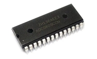
 ADC0809逐次逼近寄存器型模数转换器:资料手册参数分析

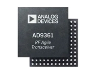
 AD9361捷变收发器:全面参数解析与关键特性概览

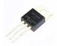
 IRF3205功率MOSFET:资料手册参数分析

 MC34063开关稳压器:全面参数解析与设计指南
