XCL205/XCL206/XCL207 Series
■ELECTRICAL CHARACTERISTICS
●XCL205A123AR/XCL206A123AR/XCL207A123AR, VOUT=1.2V, fOSC=3.0MHz, Ta=25℃
PARAMETER
SYMBOL
CONDITIONS
MIN.
TYP.
MAX. UNITS CIRCUIT
When connected to external components,
VIN=VCE=5.0V, IOUT=30mA
Output Voltage
VOUT
VIN
1.176
2.0
1.200 1.224
V
V
①
①
①
Operating Voltage Range
Maximum Output Current
-
-
6.0
-
VIN=VOUT(T)+2.0V, VCE=1.0V
IOUTMAX
600
mA
When connected to external components (*9)
V
CE=VIN,VOUT=0V,
UVLO Voltage
VUVLO
IDD
ISTB
fOSC
1.00
1.40
1.78
V
③
②
Voltage which Lx pin holding “L” level (*1, *11)
Supply Current (XCL205)
Supply Current (XCL206, XCL207)
Stand-by Current
-
-
-
46
21
0
65
35
VIN=VCE=5.0V, VOUT=VOUT(T)×1.1V
μA
VIN=5.0V, VCE=0V, VOUT=VOUT(T)×1.1V
1.0
μA
②
①
When connected to external components,
VIN=VOUT(T)+2.0V,VCE=1.0V, IOUT=100mA
Oscillation Frequency
2550
190
3000
260
3450
350
kHz
When connected to external components,
VIN=VOUT(T)+2.0V, VCE=VIN , IOUT=1mA (*12)
PFM Switching Current (*12)
IPFM
mA
⑩
PFM Duty Limit (*12)
Maximum Duty Cycle
Minimum Duty Cycle
VCE= VIN=(C-1) IOUT=1mA (*12)
-
100
-
200
300
%
%
%
①
③
③
DTYLIMIT_PFM
DMAX
VIN=VCE=5.0V, VOUT=VOUT (T)×0.9V
-
-
-
VIN=VCE=5.0V, VOUT=VOUT (T)×1.1V
0
DMIN
When connected to external components,
Efficiency
-
82
-
%
①
EFFI
RL
V
CE=VIN=VOUT (T)+1.2V, IOUT = 100mA
Lx SW "H" ON Resistance 1
Lx SW "H" ON Resistance 2
Lx SW "L" ON Resistance 1
Lx SW "L" ON Resistance 2
Lx SW "H" Leak Current (*5)
Lx SW "L" Leak Current (*5)
Current Limit (*10)
VIN=VCE=5.0V, VOUT=0V, ILX=100mA (*3)
VIN=VCE=3.6V, VOUT=0V, ILX=100mA (*3)
VIN=VCE=5.0V (*4)
-
-
-
-
-
-
0.35
0.42
0.45
0.52
0.01
0.01
1050
0.55
0.67
0.66
0.77
1.0
Ω
Ω
④
④
-
H
H
x
x
RL
RL
x
RL
x
Ω
L
L
VIN=VCE=3.6V, (*4)
Ω
-
ILeakH
ILeakL
ILIM
VIN=VOUT=5.0V, VCE=0V, LX=0V
VIN=VOUT=5.0V, VCE=0V, LX= 5.0V
VIN=VCE=5.0V, VOUT=VOUT (E)×0.9V (*8)
μA
μA
mA
⑤
⑤
⑥
1.0
900
1350
Output Voltage
Temperature Characteristics
IOUT =30mA
-40℃≦Topr≦85℃
△
VOUT/
-
±100
-
ppm/ ℃
①
③
③
(VOUT・△topr)
V
OUT=0V, Applied voltage to VCE
,
CE "H" Voltage
CE "L" Voltage
VCEH
0.65
VSS
-
-
VIN
V
V
Voltage changes Lx to “H” level (*11)
V
OUT=0V, Applied voltage to VCE,
VCEL
0.25
Voltage changes Lx to “L” level (*11)
When connected to external components,
IOUT=1mA (*6), Voltage which oscillation
frequency becomes 2550kHz≦fOSC≦3450kHz (*13)
When connected to external components,
PWM "H" Level Voltage (*13)
PWM "L" Level Voltage (*13)
VPWMH
-
-
-
VIN - 1.0
V
V
①
①
VIN
0.25
-
VPWML
I
OUT=1mA (*6), Voltage which oscillation
-
frequency becomes fOSC<2550kHz (*13)
VIN=VCE=5.0V, VOUT=0V
CE "H" Current
CE "L" Current
ICEH
ICEL
- 0.1
- 0.1
-
-
0.1
0.1
μA
μA
⑤
⑤
VIN=5.0V, VCE=0V, VOUT=0V
When connected to external components,
Soft Start Time
Latch Time
tSS
0.5
1.0
0.9
-
2.5
20
ms
ms
①
⑦
V
CE=0V→VIN , IOUT=1mA
VIN=VCE=5.0V, VOUT=0.8×VOUT
(T)
tLAT
Short Lx at 1Ω resistance (*7)
Sweeping VOUT, VIN=VCE=5.0V, Short Lx at
1Ω resistance, VOUT voltage which Lx becomes “L” 0.450
level within 1ms
Short Protection
Threshold Voltage
VSHORT
0.600
0.750
V
⑦
Inductance Value
Allowed Inductor Current
L
IDC
Test frequency=1MHz
ΔT=40℃
-
-
1.5
1000
-
-
μH
mA
Test conditions: Unless otherwise stated, VIN=5.0V, VOUT (T)=Nominal Voltage
NOTE:
*1: Including hysteresis operating voltage range.
*2: EFFI = { ( output voltage×output current ) / ( input voltage×input current) }×100
*3: ON resistance (Ω)= (VIN - Lx pin measurement voltage) / 100mA
*4: Design value
*5: When temperature is high, a current of approximately 10μA (maximum) may leak.
*6:The CE/MODE pin of the XCL207 series works also as an external switching pin of PWM control and PWM/PFM control. When the IC is in the
operation, control is switched to the automatic PWM/PFM switching mode when the CE/MODE pin voltage is equal to or greater than VIN minus
0.3V, and to the PWM mode when the CE/MODE pin voltage is equal to or lower than VIN minus 1.0V and equal to or greater than VCEH.
*7:Time until it short-circuits VOUT with GND via 1Ωof resistor from an operational state and is set to Lx=0V from current limit pulse generating.
*8: When VIN is less than 2.4V, limit current may not be reached because voltage falls caused by ON resistance.
*9: When the difference between the input and the output is small, some cycles may be skipped completely before current maximizes.
If current is further pulled from this state, output voltage will decrease because of P-ch driver ON resistance.
*10: Current limit denotes the level of detection at peak of coil current.
*11: “H”=VIN~VIN-1.2V, “L”=+0.1V~-0.1V
*12: IPFM and DTYLIMIT_PFM are defined only for the XCL206 and XCL207 series which have PFM control function. (Not for the XCL 205 series)
*13: VPWMH and VPWML are defined only for the XCL207 series. (They are not used in the XCL205/and XCL206 series)
4/26


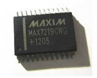
 MAX7219驱动8段数码管详解及数据手册关键信息

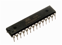
 ATMEGA328P技术资料深入分析

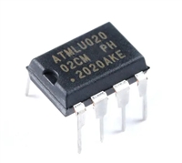
 AT24C02芯片手册管脚信息、参数分析、应用领域详解

 AT24C256芯片手册参数分析、引脚说明、读写程序示例
