W150
Pin Definitions
Pin
Pin No. Type
Pin Name
Pin Description
CPU1:2
51, 49
O
O
O
CPU Outputs 1 and 2: Frequency is set by the FS0:3 inputs or through serial input interface,
see Table 2 and Table 6. These outputs are affected by the CLK_STOP# input.
CPU_F
PCI1:5
52
Free-Running CPU Output: Frequency is set by the FS0:3 inputs or through serial input
interface, see Table 2 and Table 6. This output is not affected by the CLK_STOP# input.
11,12,13,
14, 16
PCI Outputs 1 through 5: Frequency is set by the FS0:3 inputs or through serial input
interface, see Table 2 and Table 6. These outputs are affected by the PCI_STOP# input.
PCI0/FS3
9
I/O PCI Output/Frequency Select Input: As an output, frequency is set by the FS0:3 inputs or
through serial input interface, see Table 2 and Table 6. This output is affected by the
PCI_STOP# input. When an input, latches data selecting the frequency of the CPU and PCI outputs.
PCI_F/MODE
CLK_STOP#
8
I/O Free Running PCI Output: Frequency is set by the FS0:3 inputs or through serial input
interface, see Table 2 and Table 6. This output is not affected by the PCI_STOP# input. When
an input, selects function of pin 3 as described in Table 1.
47
I
CLK_STOP# Input: When brought LOW, affected outputs are stopped LOW after completing
a full clock cycle (2–3 CPU clock latency). When brought HIGH, affected outputs start
beginning with a full clock cycle (2–3 CPU clock latency).
IOAPIC_F
IOAPIC0
54
55
29
O
O
Free-running IOAPIC Output: This output is a buffered version of the reference input which
is not affected by the CPU_STOP# logic input. Its swing is set by voltage applied to VDDQ2.
IOAPIC Output: Provides 14.318 MHz fixed frequency. The output voltage swing is set by
voltage applied to VDDQ2. This output is disabled when CLK_STOP# is set LOW.
48MHz/FS1
I/O 48 MHz Output: 48 MHz is provided in normal operation. In standard systems, this output can
be used as the reference for the Universal Serial Bus. Upon power up, FS1 input will be
latched, setting output frequencies as described in Table 2.
24MHz/FS0
REF1/FS2
30
I/O 24 MHz Output: 24 MHz is provided in normal operation. In standard systems, this output can
be used as the clock input for a Super I/O chip. Upon power up, FS0 input will be latched,
setting output frequencies as described in Table 2.
2
3
I/O Reference Output: 14.318 MHz is provided in normal operation. Upon power-up, FS2 input
will be latched, setting output frequencies as described in Table 2.
REF0
(PCI_STOP#)
I/O Fixed 14.318 MHz Output 0 or PCI_STOP# Pin: Function determined by MODE pin. The
PCI_STOP# input enables the PCI 0:5 outputs when HIGH and causes them to remain at logic
0 when LOW. The PCI_STOP signal is latched on the rising edge of PCI_F. Its effects take
place on the next PCI_F clock cycle. As an output, this pin provides a fixed clock signal equal
in frequency to the reference signal provided at the X1/X2 pins (14.318 MHz).
SDRAMIN
17
I
Buffered Input Pin: The signal provided to this input pin is buffered to 17 outputs
(SDRAM0:15, SDRAM_F).
SDRAM0:15
44, 43,
41, 40,
39, 38,
36, 35,
22, 21,
19, 18,
33, 32,
25, 24
O
Buffered Outputs: These sixteen dedicated outputs provide copies of the signal provided at
the SDRAMIN input. The swing is set by VDDQ3, and they are deactivated when CLK_STOP#
input is set LOW.
SDRAM_F
46
O
I
Free-Running Buffered Output: This output provides a single copy of the SDRAMIN input.
The swing is set by VDDQ3; this signal is unaffected by the CLK_STOP# input.
SCLK
SDATA
X1
28
27
5
Clock pin for SMBus circuitry.
I/O Data pin for SMBus circuitry.
I
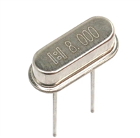
Crystal Connection or External Reference Frequency Input: This pin has dual functions.
It can be used as an external 14.318 MHz crystal connection or as an external reference
frequency input.
X2
6
I
Crystal Connection: An input connection for an external 14.318-MHz crystal. If using an
external reference, this pin must be left unconnected.
VDDQ3
1, 7, 15,
20, 31,
37, 45
P
Power Connection: Power supply for core logic, PLL circuitry, SDRAM output buffers, PCI
output buffers, reference output buffers, and 48 MHz/24 MHz output buffers. Connect to 3.3V.
Rev 1.0,November 24, 2006
Page 2 of 14


 资料手册解读:UC3842参数和管脚说明

 一文带你了解无源晶振的负载电容为何要加两颗谐振电容CL1和CL2

 玻璃管保险丝与陶瓷管保险丝:区别与替代性探讨

 PCF8574资料解读:主要参数分析、引脚说明
