
 5秒后页面跳转

| 是否Rohs认证: | 符合 | 生命周期: | Obsolete |
| 包装说明: | 13 X 15 MM, LEAD FREE, PLASTIC, BGA-165 | Reach Compliance Code: | compliant |
| 风险等级: | 5.84 | 最长访问时间: | 0.45 ns |
| 最大时钟频率 (fCLK): | 250 MHz | I/O 类型: | COMMON |
| JESD-30 代码: | R-PBGA-B165 | 长度: | 15 mm |
| 内存密度: | 18874368 bit | 内存集成电路类型: | DDR SRAM |
| 内存宽度: | 18 | 功能数量: | 1 |
| 端子数量: | 165 | 字数: | 1048576 words |
| 字数代码: | 1000000 | 工作模式: | SYNCHRONOUS |
| 最高工作温度: | 85 °C | 最低工作温度: | -40 °C |
| 组织: | 1MX18 | 输出特性: | 3-STATE |
| 封装主体材料: | PLASTIC/EPOXY | 封装代码: | LBGA |
| 封装等效代码: | BGA165,11X15,40 | 封装形状: | RECTANGULAR |
| 封装形式: | GRID ARRAY, LOW PROFILE | 并行/串行: | PARALLEL |
| 电源: | 1.5/1.8,1.8 V | 认证状态: | Not Qualified |
| 座面最大高度: | 1.46 mm | 最大待机电流: | 0.5 A |
| 最小待机电流: | 1.7 V | 子类别: | SRAMs |
| 最大压摆率: | 0.52 mA | 最大供电电压 (Vsup): | 1.9 V |
| 最小供电电压 (Vsup): | 1.7 V | 标称供电电压 (Vsup): | 1.8 V |
| 表面贴装: | YES | 技术: | CMOS |
| 温度等级: | INDUSTRIAL | 端子形式: | BALL |
| 端子节距: | 1 mm | 端子位置: | BOTTOM |
| 宽度: | 13 mm | Base Number Matches: | 1 |
| 型号 | 品牌 | 描述 | 获取价格 | 数据表 |
| UPD46184184BF1-E40Y-EQ1-A | RENESAS | DDR SRAM |
获取价格 |

|
| UPD46184185BF1-E33-EQ1 | RENESAS | DDR SRAM |
获取价格 |
|
| UPD46184185BF1-E33Y-EQ1-A | RENESAS | UPD46184185BF1-E33Y-EQ1-A |
获取价格 |
|
| UPD46184185BF1-E40-EQ1-A | RENESAS | UPD46184185BF1-E40-EQ1-A |
获取价格 |
|
| UPD46184185BF1-E40Y-EQ1-A | RENESAS | QDRII/DDRII/ QDRII+/DDRII+ SRAM, LBGA, /Tray |
获取价格 |
|
| UPD46184362BF1-E33-EQ1 | RENESAS | DDR SRAM |
获取价格 |
|
 MAX3485芯片手册参数分析及替代型号推荐

 ADXL345传感器工作原理、参数分析、引脚说明
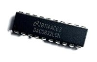 一文带你了解,DAC0832工作原理、输出电压范围、分辨率等参数
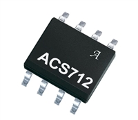 ACS712电流检测使用指南及资料手册参数分析
工作时间:9:00-21:00
CEO邮箱:ceo@jiepei.com
投诉邮箱:tousu@jiepei.com


 浙公网安备 33010502006866号 浙ICP备10014259号-119
营业执照ICP证
浙公网安备 33010502006866号 浙ICP备10014259号-119
营业执照ICP证


