TPSM846C24
ZHCSHH6B –JANUARY 2018–REVISED JANUARY 2019
www.ti.com.cn
Pin Functions
PIN
I/O
DESCRIPTION
NAME
NO.
10
AGND
G
G
Analog ground for the controller circuitry. This pin is internally connected to PGND.
Return path for VINBP and BP3. This pin is internally connected to PGND, pad 59.
BP_RTN
51
Output of the internal 3.3-V regulator. Bypass this pin with a minimum of 2.2-µF to BP_RTN.
Can be used as a pullup termination voltage for PGOOD and EN signals.
BP3
BP6
47
49
O
O
Output of the internal 6.5-V regulator that powers the driver stage of the device. Bypass this
pin with a minimum of 2.2 µF to BP6_RTN.
BP6_RTN
COMP
48
9
G
O
Power ground return path for BP6 bypass cap.
Output of the error amplifier.
Output of the remote sense differential amplifier. This provides remote sensing for output
voltage reporting and the voltage control loop.
DIFFO
DNC
EN
6
O
–
I
Do Not Connect. Do not connect these pins to AGND, PGND to a different DNC pin or to any
other voltage. These pins are connected to internal circuitry. Each pin must be soldered to an
isolated pad.
8, 16, 17, 18,
19, 20, 21, 30, 31
EN pin. To enable, pull this pin up to a voltage less than 5.5 V using a 10-kΩ resistor. Pull this
pin to AGND to disable the device.
12
FB
7
2
I
I
Feedback pin for the control loop.
ISHARE
Current sharing signal for parallel operation.
Not Connected. These pins are internally isolated from any signal and all other pins. Each pin
must be soldered to a pad on the PCB. These pins can be left isolated, or connected to AGND
or PGND.
NC
1, 15
–
Power ground of the device. This is the return current path for the power stage of the device.
Connect these pins to the bypass capacitors associated with VIN and VOUT. Connect pads
56, 57, 58, and 59 to the PCB ground planes using multiple vias for optimal thermal
performance. All pins must be connected together externally with a copper plane or pour
directly under the device.
32, 33, 34, 35
36, 42, 43, 54
56, 57, 58, 59
PGND
G
Power-good indicator. This pin is an open-drain output, which asserts low during any fault
conditions. Requires a pullup resistor.
PGOOD
PH
52
O
O
22, 23, 24, 25
26, 27, 28, 29
Phase switch node. Do not connect any external components to these pins or tie them to a pin
of a different function.
Frequency-setting resistor. To operate the device at its default switching frequency, make no
connection to this pin. To operate at a different switching frequency, connect a resistor from
this pin to AGND.
RT
13
14
I
I
RT resistor select. To operate the device at its default switching frequency, connect this pin to
AGND. To operate at a different switching frequency, let this pin float.
RT_SEL
Frequency synchronization pin. In a stand-alone application or as the Master device in a
parallel configuration, the SYNC pin is configured as a SYNC-IN pin and power conversion is
synchronized to the rising edge of a 50% duty cycle external clock applied to this pin.
For a slave device in a parallel configuration, power conversion is synchronized to the falling
edge of the incoming clock.
SYNC
11
I/O
VIN
44, 45, 46, 53
50
I
I
Input switching voltage pins. These pins supply voltage to the power switches of the converter.
Input power to the controller circuitry. Bypass this pin with a minimum of 1-µF to BP_RTN. This
pin is internally connected to VIN.
VINBP
37, 38, 39,
40, 41, 55
Output voltage. These pins are connected to the internal output inductor. Connect these pins
to the output load and connect external bypass capacitors between these pins and PGND.
VOUT
VS+
O
I
Positive input of the remote sense amplifier. Connect this pin to VOUT at the load for best
voltage regulation. Do not let this pin float.
4
Negative input of the remote sense amplifier. Connect this pin to ground at the load for best
voltage regulation. Do not let this pin float.
VS–
5
3
I
VSHARE
I/O
Voltage sharing signal for parallel operation.
4
Copyright © 2018–2019, Texas Instruments Incorporated


 压敏电阻器在直流电路中的过压保护应用探讨

 电感耐压值及其与电感大小的关系

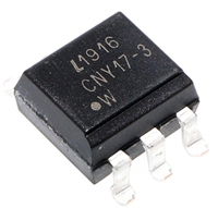
 CNY17F光耦合器:特性、应用、封装、引脚功能及替换型号解析

 DS1307资料解析:特性、引脚说明、替代推荐
