TH7426A/27A
V
This is the output amplifier power supply (high side). It also supplies the “Read Enable” switching device which ex-
plains that I is different whether RE is at high or low level.
DD
DD
G
This is the output amplifier low side power supply. G
is linked to V
through a diode, G
being the cathode
ND
ND
ND
SS
node. Thus G
must always be more positive than or equal to Vss.
ND
It must be noticed that “RE” switching device is powered from V
to V . G
is specific to output amplifier.
ND
DD
SS
V
V
This is the amplifier output.
OS
SS
S
This is the CCD multiplexor substrate bias. All applied biases and clock levels must be more positive or equal to V
.
SS
T
These are the internal temperature sensor connections. Temperature sensor is floating with respect to all other pin
connections. Pins 3 to 6 are internally connected together as well as pin 80 to 83.
TC+ This is the internal thermoelectric cooler positive input (current enters) (all pins must be externally connected in or-
der to lower current density into each pin).
TC-
This is the internal thermoelectric cooler negative input (current goes out). Thermoelectric cooler connections are
floating, with respect to all other pins. All pins must be externally connected in order to lower individual pin current
density. It is advised to avoid pulsed current regulations to drive TE cooler, since it may result in EMC troubleshoo-
ting inside component cavity.
FUNCTIONAL DESCRIPTION
Individual InGaAs diodes are reversed bias. The cathode node is common to all diodes and connected to a fixed potential
Vn. The anode of each diode is wire bonded to a lateral entrance of the readout CCD stage.
These diodes behave as capacitors whose leakage current depends on dark current and illumination. This current tends to
decrease the voltage across the capacitor. Each diode capacity is first preloaded with a calibrated amount of negative char-
ges (Qb). After an integration time (TI), the amount of removed charges (QI) figures out the cumulated light absorption. So
the measurement of the remaining charge amount (Qs) in the diode capacitor gives access to QI (QI = Qb - Qs). This is
called “Vidicon” readout mode.
CCD multiplexors fulfill all those operations. They provide preloading and readout functions for the separate odd and even
pixel groups. The main CCD features consist in a two phase register (φ and φ ) with longitudinal and lateral transfer ca-
L1
L2
pability. Following is a description of how those devices keep photodiodes under control and capture pixel signals.
Four main functions can be considered :
- Preload
The potential gap between the two gates [V
and spilling occurs using an injection diode φ
-V
] defines a potential well for preload calibration (Qb), its filling
GL1 GL2
.
PL
- Main register charge handling
At each individual transfer step, Qs moves out of the 150th stage, while Qb moves in the first stage. The longitudinal
register stage requires a series of at least 150 steps to complete the preloading cycle. This transfer operation is inhi-
bited if RE (read enable) input is maintained at a low level.
- Photodiode information collection (and reset)
The lateral input stage consists in 150 input diodes, each of them directly wire bonded to one photodiode, and con-
trolled under a single common biasing gate V
and a lateral transfer gate φ .
G1
x
At the end of integration time (see timing diagram Figure 1) :
- the preload charges Qb, stored in the register, are transferred simultaneously to the 150 photodiodes when φ is at
x
high level and φ at low level, allowing the photodiode reset.
L1
- charges in excess (identified as Qs) are collected back to the register by forcing φ at high level. At this step the
L1
register current information is the mirror image of the collected photo signal and, all photodiodes are reseted while a
new TI starts.
To isolate each stage from the other one, φ must be at low level during all lateral transfer operations.
L2
- Data read-out
At the end of the photodiode reset operation :
- if RE is forced to low level (Timing Diagram - Figure 1), all Qs information remain stored in the register and so, rea-
dout is delayed .According to this situation a next photodiode reset procedure can’t be operated until the full longitu-
dinal transfer takes place (150 steps minimum).
6/20


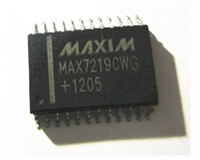
 MAX7219驱动8段数码管详解及数据手册关键信息

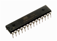
 ATMEGA328P技术资料深入分析

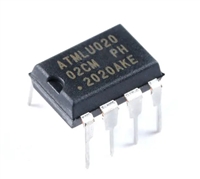
 AT24C02芯片手册管脚信息、参数分析、应用领域详解

 AT24C256芯片手册参数分析、引脚说明、读写程序示例
