TEST LEVEL
TEST PROCEDURE
TEST LEVEL CODES
All electrical characteristics are subject to the
following conditions:
I
100% production tested at the specified temperature.
II
100% production tested at T =25 °C, and sample
A
tested at the specified temperatures.
All parameters having min/max specifications
are guaranteed. The Test Level column indi-
cates the specific device testing actually per-
formed during production and Quality Assur-
ance inspection. Any blank section in the data
column indicates that the specification is not
tested at the specified condition.
III
QA sample tested only at the specified temperatures.
IV
Parameter is guaranteed (but not tested) by design
and characterization data.
V
Parameter is a typical value for information purposes
only.
VI
100% production tested at T = 25 °C. Parameter is
A
guaranteed over specified temperature range.
The leading edge of the input signal (which consists of a
20 mV overdrive voltage) changes the comparator output
TIMING INFORMATION
after a time of t
or t
(Q or ). The input signal must be
Q
pdH
s
pdL
The timing diagram for the comparator is shown in figure 1.
If LE is high and low in the SPT9689, the comparator
maintained for a time t (set-up time) before the LE falling
LE
tracks the input difference voltage. When LE is driven low
and high, the comparator outputs are latched into their
edge and
rising edge and held for time t after the falling
H
LE
edge for the comparator to accept data. After t , the output
ignores the input status until the latch is strobed again. A
minimum latch pulse width of t is needed for strobe
H
LE
existing logic states.
pL
operation, and the output transitions occur after a time of
t
or t
.
pLOH
pLOL
Figure 1 - Timing Diagram
Latch Enable
Latch Enable
50%
tH
tpL
tS
Differential
Input Voltage
V
± V
OS
REF
50%
50%
V
OD
tpLOH
t pdL
Output Q
Output Q
tpdH
tpLOL
V
+=100 mV (p-p), V
=20 mV
OD
IN
The set-up and hold times are a measure of the time required for an input signal to propagate through the
first stage of the comparator to reach the latching circuitry. Input signals occurring before t will be detected
s
and held; those occurring after t will not be detected. Changes between t and t may not be detected.
H
s
H
SPT9689
SPT
3
7/17/00


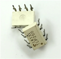
 TLP250光耦合器:资料手册参数分析

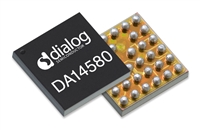
 DA14580 低功耗蓝牙系统级芯片(SoC):资料手册参数分析

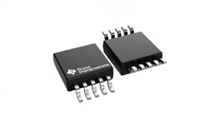
 INA226 高精度电流和功率监控器:资料手册参数分析

 SI2302 N沟道MOSFET:资料手册参数分析
