
| 是否无铅: | 不含铅 | 是否Rohs认证: | 符合 |
| 生命周期: | Active | 零件包装代码: | SOIC |
| 包装说明: | SOIC-14 | 针数: | 14 |
| Reach Compliance Code: | compliant | ECCN代码: | EAR99 |
| HTS代码: | 8542.39.00.01 | Factory Lead Time: | 1 week |
| 风险等级: | 0.69 | Samacsys Confidence: | 3 |
| Samacsys Status: | Released | Samacsys PartID: | 181732 |
| Samacsys Pin Count: | 14 | Samacsys Part Category: | Integrated Circuit |
| Samacsys Package Category: | Small Outline Packages | Samacsys Footprint Name: | D(R-PDSO-G14) |
| Samacsys Released Date: | 2015-04-13 16:56:13 | Is Samacsys: | N |
| 差分输出: | YES | 驱动器位数: | 1 |
| 高电平输入电流最大值: | 0.0001 A | 输入特性: | DIFFERENTIAL SCHMITT TRIGGER |
| 接口集成电路类型: | LINE TRANSCEIVER | 接口标准: | EIA-485-A; TIA-485-A; ISO 8482 |
| JESD-30 代码: | R-PDSO-G14 | JESD-609代码: | e4 |
| 长度: | 8.65 mm | 湿度敏感等级: | 1 |
| 功能数量: | 1 | 端子数量: | 14 |
| 最高工作温度: | 85 °C | 最低工作温度: | -40 °C |
| 最小输出摆幅: | 1 V | 输出特性: | DIFFERENTIAL |
| 最大输出低电流: | 0.0001 A | 输出极性: | COMPLEMENTARY |
| 封装主体材料: | PLASTIC/EPOXY | 封装代码: | SOP |
| 封装等效代码: | SOP14,.25 | 封装形状: | RECTANGULAR |
| 封装形式: | SMALL OUTLINE | 峰值回流温度(摄氏度): | 260 |
| 电源: | 5 V | 认证状态: | Not Qualified |
| 最大接收延迟: | 20 ns | 接收器位数: | 1 |
| 座面最大高度: | 1.75 mm | 子类别: | Line Driver or Receivers |
| 最大压摆率: | 15 mA | 最大供电电压: | 5.25 V |
| 最小供电电压: | 4.75 V | 标称供电电压: | 5 V |
| 电源电压1-最大: | 5.25 V | 电源电压1-分钟: | 4.75 V |
| 电源电压1-Nom: | 5 V | 表面贴装: | YES |
| 技术: | BICMOS | 温度等级: | INDUSTRIAL |
| 端子面层: | Nickel/Palladium/Gold (Ni/Pd/Au) | 端子形式: | GULL WING |
| 端子节距: | 1.27 mm | 端子位置: | DUAL |
| 处于峰值回流温度下的最长时间: | NOT SPECIFIED | 最大传输延迟: | 12 ns |
| 宽度: | 3.9 mm | Base Number Matches: | 1 |
| 型号 | 品牌 | 替代类型 | 描述 | 数据表 |
| SN65LBC180ADR | TI |
完全替代  |
LOW POWER DIFFERENTIAL LINE DRIVER AND RECEIVER PAIRS |

|
| SN75LBC180AD | TI |
类似代替 |
LOW POWER DIFFERENTIAL LINE DRIVER AND RECEIVER PAIRS |
|
| SN65LBC180DR | TI |
类似代替 |
LOW-POWER RS-485 LINE DRIVER AND RECEIVER PAIRS |
|
| 型号 | 品牌 | 获取价格 | 描述 | 数据表 |
| SN65LBC180ADG4 | TI |
获取价格 |
低功耗差分线路驱动器和接收器对 | D | 14 | -40 to 85 |
|
| SN65LBC180ADR | TI |
获取价格 |
LOW POWER DIFFERENTIAL LINE DRIVER AND RECEIVER PAIRS |
|
| SN65LBC180ADRG4 | TI |
获取价格 |
Low-Power Differential Line Driver And Receiver Pair 14-SOIC -40 to 85 |
|
| SN65LBC180AN | TI |
获取价格 |
LOW POWER DIFFERENTIAL LINE DRIVER AND RECEIVER PAIRS |
|
| SN65LBC180ANE4 | TI |
获取价格 |
LINE TRANSCEIVER, PDIP14, ROHS COMPLIANT, PLASTIC, MS-001AA, DIP-14 |
|
| SN65LBC180AP | TI |
获取价格 |
LINE TRANSCEIVER, PDIP14, PLASTIC, DIP-14 |
|
| SN65LBC180D | TI |
获取价格 |
LOW-POWER DIFFERENTIAL LINE DRIVER AND RECEIVER PAIRS |
|
| SN65LBC180DG4 | TI |
获取价格 |
LOW-POWER RS-485 LINE DRIVER AND RECEIVER PAIRS |
|
| SN65LBC180DR | TI |
获取价格 |
LOW-POWER RS-485 LINE DRIVER AND RECEIVER PAIRS |
|
| SN65LBC180DRG4 | TI |
获取价格 |
LOW-POWER RS-485 LINE DRIVER AND RECEIVER PAIRS |
|
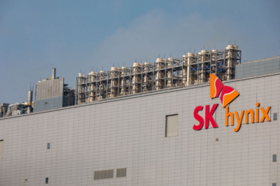 突破性进展!SK海力士全球首发量产型High NA EUV设备及高效散热DRAM

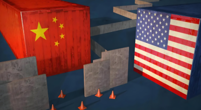 美国再次按下暂停键:GPU关税豁免3个月背后暗藏怎样的半导体
 宇树科技冲刺IPO,"杭州六小龙"即将登陆资本市场?
 台积电酝酿高端芯片涨价潮!苹果英伟达或面临成本压力
工作时间:9:00-21:00
CEO邮箱:ceo@jiepei.com
投诉邮箱:tousu@jiepei.com


 浙公网安备 33010502006866号 浙ICP备10014259号-119
营业执照ICP证
浙公网安备 33010502006866号 浙ICP备10014259号-119
营业执照ICP证


