
 5秒后页面跳转

| Status: | Active | Vin (min) (V): | 4.5 |
| Vin (max) (V): | 28 | Battery Charge Voltage (max) (V): | 22 |
| Battery Charge Current (max) (A): | 2 | Input Source: | AC Adapter;USB |
| Features: | Adjustable Current Limit;Adjustable Soft-Start;Enable Input;OCP;UVP | Package Type: | WQFN4x4-24 |
| 型号 | 品牌 | 获取价格 | 描述 | 数据表 |
| RT9535A | RICHTEK |
获取价格 |
暂无描述 |

|
| RT9535B | RICHTEK |
获取价格 |
暂无描述 |
|
| RT9536 | RICHTEK |
获取价格 |
暂无描述 |
|
| RT9536H | RICHTEK |
获取价格 |
暂无描述 |
|
| RT9538 | RICHTEK |
获取价格 |
暂无描述 |
|
| RT9541 | ETC |
获取价格 |
LI LON BATTERY PROTECTOR |
|
| RT9541ACE | ETC |
获取价格 |
LI LON BATTERY PROTECTOR |
|
| RT9541ACER | ETC |
获取价格 |
LI LON BATTERY PROTECTOR |
|
| RT9541BCE | ETC |
获取价格 |
LI LON BATTERY PROTECTOR |
|
| RT9541BCER | ETC |
获取价格 |
LI LON BATTERY PROTECTOR |
|
 解析BAV99LT1G手册:参数分析、替换型号推荐

 解读BSS138PW数据手册:产品特性、电气参数及替换型号推荐
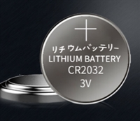 CR2032资料手册解读:参数分析、替换型号推荐
 CDSOT23-SM712参数分析、替代型号推荐
工作时间:9:00-21:00
CEO邮箱:ceo@jiepei.com
投诉邮箱:tousu@jiepei.com


 浙公网安备 33010502006866号 浙ICP备10014259号-119
营业执照ICP证
浙公网安备 33010502006866号 浙ICP备10014259号-119
营业执照ICP证


