
 5秒后页面跳转

| 型号 | 品牌 | 获取价格 | 描述 | 数据表 |
| RT9108N | RICHTEK |
获取价格 |
15W Stereo Class-D Audio Power Amplifier |

|
| RT9108NL | RICHTEK |
获取价格 |
9W Stereo Class-D Audio Power Amplifier |
|
| RT9114B | RICHTEK |
获取价格 |
暂无描述 |
|
| RT9114C | RICHTEK |
获取价格 |
Dual Channel Digital Audio System with EQ and Frequency DRC Control |
|
| RT9116 | RICHTEK |
获取价格 |
暂无描述 |
|
| RT9118 | RICHTEK |
获取价格 |
暂无描述 |
|
| RT9120 | RICHTEK |
获取价格 |
20W, Stereo, Inductor-Less I2S-Input, Low Noise, High-Efficiency Closed-Loop General-Purpo |
|
| RT9-1203R20D1 | RSG |
获取价格 |
DC/DC-Converter |
|
| RT9-1205R20D1 | RSG |
获取价格 |
DC/DC-Converter |
|
| RT9-1205RD20D1 | RSG |
获取价格 |
DC/DC-Converter |
|
 US1M数据手册解读:产品特性、替换型号推荐

 解析BAV99LT1G手册:参数分析、替换型号推荐
 解读BSS138PW数据手册:产品特性、电气参数及替换型号推荐
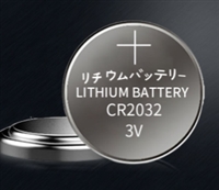 CR2032资料手册解读:参数分析、替换型号推荐
工作时间:9:00-21:00
CEO邮箱:ceo@jiepei.com
投诉邮箱:tousu@jiepei.com


 浙公网安备 33010502006866号 浙ICP备10014259号-119
营业执照ICP证
浙公网安备 33010502006866号 浙ICP备10014259号-119
营业执照ICP证


