
 5秒后页面跳转

| 型号 | 品牌 | 获取价格 | 描述 | 数据表 |
| MC10EL12D | ONSEMI |
获取价格 |
5.0 V ECL Low Impedance Driver |

|
| MC10EL12D | MOTOROLA |
获取价格 |
Low Impedance Drive |
|
| MC10EL12DG | ONSEMI |
获取价格 |
5.0 V ECL Low Impedance Driver |
|
| MC10EL12DR2 | ONSEMI |
获取价格 |
5.0 V ECL Low Impedance Driver |
|
| MC10EL12DR2G | ONSEMI |
获取价格 |
5.0 V ECL Low Impedance Driver |
|
| MC10EL12DT | ONSEMI |
获取价格 |
5.0 V ECL Low Impedance Driver |
|
| MC10EL12DTG | ONSEMI |
获取价格 |
5.0 V ECL Low Impedance Driver |
|
| MC10EL12DTR2 | ONSEMI |
获取价格 |
5.0 V ECL Low Impedance Driver |
|
| MC10EL12DTR2G | ONSEMI |
获取价格 |
5.0 V ECL Low Impedance Driver |
|
| MC10EL12MNR4 | ONSEMI |
获取价格 |
5.0 V ECL Low Impedance Driver |
|
 RF5110数据手册详解:3V GSM射频功率放大器的深度分析

 REF1004-1.2手册详解:引脚信息、产品描述、参数分析
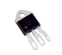 晶闸管的静态特性与伏安特性详解
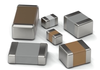 贴片电容的工作原理与参数识别
工作时间:9:00-21:00
CEO邮箱:ceo@jiepei.com
投诉邮箱:tousu@jiepei.com


 浙公网安备 33010502006866号 浙ICP备10014259号-119
营业执照ICP证
浙公网安备 33010502006866号 浙ICP备10014259号-119
营业执照ICP证


