Mono/Stereo High-Power Class D Amplifier
ABSOLUTE MAXIMUM RATINGS
PVDD to PGND.......................................................-0.3V to +30V
AGND to PGND.....................................................-0.3V to +0.3V
Continuous Power Dissipation (T = +70°C)
A
32-Pin TQFN Single-Layer PCB
INL, INR, FBL, FBR, COM to AGND.........-0.3V to (V
+ 0.3V)
REG
MUTE, SHDN, MONO, MOD, REGEN to AGND.......-0.3V to +6V
REG to AGND ..............................................-0.3V to (VS + 0.3V)
VS to AGND (Note 1)................................................-0.3V to +6V
OUTL+, OUTL-, OUTR+,
OUTR-, to PGND...................................-0.3V to (PVDD + 0.3V)
C1N to PGND ..........................................-0.3V to (PVDD + 0.3V)
(derate 37mW/°C above +70°C).....................................2.96W
θ
JC
...................................................................................27°C/W
....................................................................................1°C/W
JA
θ
MAX9736
C1P to PGND ...........................(PVDD - 0.3V) to (V
+ 0.3V)
BOOT
BOOT to PGND ............................................(V
OUTL+, OUTL-, OUTR+, OUTR-,
- 0.3V) to 36V
Operating Temperature Range ...........................-40°C to +85°C
Storage Temperature Range.............................-65°C to +150°C
Junction Temperature......................................................+150°C
Lead Temperature (soldering, 10s) .................................+300°C
C1P
Short Circuit to PGND or PVDD...............................Continuous
Thermal Limits (Notes 2, 3)
Note 1: VS cannot exceed PVDD + 0.3V. See the Power Sequencing section.
Note 2: Thermal performance of this device is highly dependant on PCB layout. See the Applications Information section for more details.
Note 3: Package thermal resistances were obtained using the method described in JEDEC specification JESD51-7, using a 4-layer
board. For detailed information on package thermal considerations, visit www.maxim-ic.com/thermal-tutorial.
Stresses beyond those listed under “Absolute Maximum Ratings” may cause permanent damage to the device. These are stress ratings only, and functional
operation of the device at these or any other conditions beyond those indicated in the operational sections of the specifications is not implied. Exposure to
absolute maximum rating conditions for extended periods may affect device reliability.
ELECTRICAL CHARACTERISTICS
(V
= 20V, V = 5V, AGND = PGND = 0V, V
= V
= V
= 5V, REGEN = MONO = AGND, C1 = 0.1µF, C2 = 1µF,
MUTE
PVDD
VS
MOD
SHDN
R
_ = 20kΩ and R = 20kΩ, R = ∞, AC measurement bandwidth 22Hz to 22kHz, T = T
to T
, unless otherwise noted.
IN
FB_
L
A
MIN
MAX
Typical values are at T = +25°C.) (Notes 4, 5)
A
PARAMETER
SYMBOL
CONDITIONS
MIN
TYP
MAX
UNITS
AMPLIFIER DC CHARACTERISTICS
Speaker Supply Voltage Range
PVDD
VS
Inferred from PSRR test
(Notes 1 and 7)
8
28
V
V
Preamplifier Supply Voltage
Range
4.5
5.5
Undervoltage Lockout
UVLO
7
V
T
T
T
T
= +25°C
30
45
50
20
22
10
10
A
A
A
A
R = ∞, V
= 5V,
= 0V,
L
REGEN
REGEN
I
mA
PVDD
V
= open
VS
= T
to T
MIN
MAX
MAX
Quiescent Supply Current
= +25°C
= T to T
14
1
R = ∞, V
L
I
VS
mA
µA
V
= 5V
VS
MIN
I
I
PVDD
VS
Shutdown Supply Current
I
V
= 0V
SHDN
SHDN
REG Voltage
V
4.2
4.8
V
V
V
REG
Preregulator Voltage
COM Voltage
VS
Internal regulated 5V, V = 5V
REGEN
V
1.9
2.05
2.2
COM
INPUT AMPLIFIER CHARACTERISTICS
Capacitive Drive
C
30
2
pF
V
L
Output Swing (Note 6)
Sinking 1mA
Open-Loop Gain
A
V
V
= V
500mV, R = 20kΩ to IN_
88
1
dB
VO
FB_
COM
FB_
Input Offset Voltage
mV
OS
2
_______________________________________________________________________________________


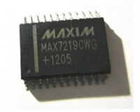
 MAX7219驱动8段数码管详解及数据手册关键信息

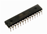
 ATMEGA328P技术资料深入分析

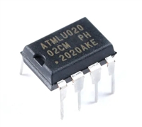
 AT24C02芯片手册管脚信息、参数分析、应用领域详解

 AT24C256芯片手册参数分析、引脚说明、读写程序示例
