
 5秒后页面跳转

| 型号 | 品牌 | 描述 | 获取价格 | 数据表 |
| MAX9311ECJ | MAXIM | 1:10 Differential LVPECL/LVECL/HSTL Clock and Data Drivers |
获取价格 |

|
| MAX9311ECJ+T | MAXIM | Clock Driver, 10 True Output(s), 0 Inverted Output(s), PQFP32, 7 X 7 MM, LQFP-32 |
获取价格 |
|
| MAX9311ECJ-T | MAXIM | Low Skew Clock Driver, 9311 Series, 10 True Output(s), 0 Inverted Output(s), PQFP32, 7 X 7 |
获取价格 |
|
| MAX9311EGJ | MAXIM | 1:10 Differential LVPECL/LVECL/HSTL Clock and Data Drivers |
获取价格 |
|
| MAX9311EGJ-T | MAXIM | Low Skew Clock Driver, 9311 Series, 10 True Output(s), 0 Inverted Output(s), 5 X 5 MM, 0.9 |
获取价格 |
|
| MAX9311EHJ | MAXIM | 1:10 Differential LVPECL/LVECL/HSTL Clock and Data Drivers |
获取价格 |
|
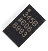 ADXL345传感器工作原理、参数分析、引脚说明

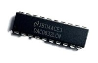 一文带你了解,DAC0832工作原理、输出电压范围、分辨率等参数
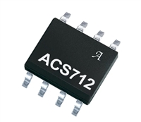 ACS712电流检测使用指南及资料手册参数分析
 TLP521资料手册解读:参数分析、引脚说明、典型电路
工作时间:9:00-21:00
CEO邮箱:ceo@jiepei.com
投诉邮箱:tousu@jiepei.com


 浙公网安备 33010502006866号 浙ICP备10014259号-119
营业执照ICP证
浙公网安备 33010502006866号 浙ICP备10014259号-119
营业执照ICP证


