LTC7862
ELECTRICAL CHARACTERISTICS The l denotes the specifications which apply over the specified operating
junction temperature range, otherwise specifications are at TA = 25°C (Note 2), VIN = 12V, VRUN = 5V, VEXTVCC = 0V, VDRVUV = 0V
unless otherwise noted.
SYMBOL
PARAMETER
CONDITIONS
MIN
TYP
MAX
UNITS
Fault Timer and WARNB Output
l
l
l
l
I
I
I
TMR Pull-Up Current (Switching)
TMR Pull-Down Current (Dropout)
TMR Pull-Down Current (Cool-Down)
TMR Switching Off Threshold
TMR Retry Threshold
TMR = 0V, V = 0.83V
–35
0.7
–40
1.1
–45
1.4
µA
µA
SWITCHING
FB
TMR = 1V, V = 0.77V
DROPOUT
FB
TMR = 2.5V
0.7
1.1
1.4
µA
COOLDOWN
2.13
0.19
52
2.19
0.25
55
2.23
0.31
58
V
V
TMR Switching Set Time
(Initial Fault Period) per 1µF
ms/µF
TMR Switching Set Time
(Retry Period) per 1µF
50
ms/µF
TMR Cool-Down Time per 1µF
Retry Duty Cycle During a Sustained Fault
WARNB Voltage Low
1700
2.7
ms/µF
%
D
1.8
3.5
0.04
10
RETRY
WARNB
WARNB
WARNB
V
I
= 2mA
= 3.3V
0.02
V
WARNB
I
t
WARNB Leakage Current
V
µA
WARNB
Delay from TG Going High to WARNB
Going High Impedance
60
µs
Note 1: Stresses beyond those listed under Absolute Maximum Ratings
may cause permanent damage to the device. Exposure to any Absolute
Maximum Ratings for extended periods may affect device reliability and
lifetime.
Note 4: The LTC7862 is tested in a feedback loop that servos V to a
ITH
specified voltage and measures the resultant V . The specification at
FB
85°C is not tested in production and is assured by design, characterization
and correlation to production testing at other temperatures (125°C for the
LTC7862E and LTC7862I, 150°C for the LTC7862H). For the LTC7862I
and LTC7862H, the specification at 0°C is not tested in production and is
assured by design, characterization and correlation to production testing
at –40°C.
Note 5: Dynamic supply current is higher due to the gate charge being
delivered at the switching frequency. See the Applications Information
section.
Note 2: The LTC7862 is tested under pulsed load conditions such that T ≈
J
T . The LTC7862E is guaranteed to meet performance specifications from
A
0°C to 85°C. Specifications over the –40°C to 125°C operating junction
temperature range are assured by design, characterization and correlation
with statistical process controls. The LTC7862I is guaranteed over the
–40°C to 125°C operating junction temperature range and the LTC7862H
is guaranteed over the –40°C to 150°C operating junction temperature
range. Note that the maximum ambient temperature consistent with
these specifications is determined by specific operating conditions in
conjunction with board layout, the rated package thermal impedance
and other environmental factors. High temperatures degrade operating
lifetimes; operating lifetime is derated for junction temperatures greater
Note 6: Rise and fall times are measured using 10% and 90% levels.
Delay times are measured using 50% levels.
Note 7: The minimum on-time condition is specified for an inductor
peak-to-peak ripple current >40% of I
(See Minimum On-Time
MAX
Considerations in the Applications Information section).
than 125ºC. The junction temperature (T , in °C) is calculated from the
J
Note 8: Do not apply a voltage or current source to these pins. They must
be connected to capacitive loads only, otherwise permanent damage may
occur.
ambient temperature (T , in °C) and power dissipation (P , in Watts)
A
D
according to the formula:
T = T + (P • θ )
JA
J
A
D
Note 9: The minimum input supply operating range is dependent on the
where θ = 38°C/W for the TSSOP package and θ = 43°C/W for the
DRV UVLO thresholds as determined by the DRVUV pin setting.
JA
JA
CC
QFN package.
Note 10: All voltages with respect to GND unless otherwise noted. Positive
currents are into pins; negative currents are out of pins unless otherwise
noted.
Note 3: This IC includes overtemperature protection that is intended to
protect the device during momentary overload conditions. The maximum
rated junction temperature will be exceeded when this protection is active.
Continuous operation above the specified absolute maximum operating
junction temperature may impair device reliability or permanently damage
the device.
Rev 0
5
For more information www.analog.com


 压敏电阻器在直流电路中的过压保护应用探讨

 电感耐压值及其与电感大小的关系

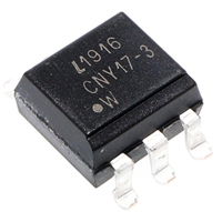
 CNY17F光耦合器:特性、应用、封装、引脚功能及替换型号解析

 DS1307资料解析:特性、引脚说明、替代推荐
