Absolute Maximum Ratings
b
a
65 C to 150 C
If Military/Aerospace specified devices are required,
please contact the National Semiconductor Sales
Office/Distributors for availability and specifications.
(Note 6)
Storage Temperature Range
§
§
Lead Temperature (Soldering, 10 sec.)
260 C
§
Soldering Information
Dual-In-Line Package
Soldering (10 sec.)
Small Outline Package
Vapor Phase (60 sec.)
Infrared (15 sec.)
g
Supply Voltage
18V
260 C
§
Power Dissipation (Note 1)
Input Voltage (Note 2)
500 mW
215 C
§
g
15V
220 C
§
Output Short Circuit Duration (Note 3)
Indefinite
See AN-450 ‘‘Surface Mounting Methods and Their Effect
on Product Reliability’’ for other methods of soldering sur-
face mount devices.
Operating Temperature Range
b
b
a
55 C to 125 C
LM110
LM210
LM310
§
25 C to 85 C
§
a
§
§
ESD rating to be determined.
a
0 C to 70 C
§
§
Electrical Characteristics (Note 4)
LM110
Typ
1.5
LM210
Typ
1.5
LM310
Typ
2.5
Parameter
Conditions
Units
Min
Max Min
Max Min
Max
7.5
e
e
e
Input Offset Voltage
Input Bias Current
Input Resistance
Input Capacitance
T
A
T
A
T
A
25 C
§
4.0
3.0
4.0
3.0
mV
nA
X
25 C
§
1.0
1.0
2.0
7.0
10
12
10
12
10
10
10
12
25 C
§
10
10
10
10
1.5
1.5
1.5
pF
e
e
g
Large Signal Voltage
Gain
T
25 C, V
§
15V
A
S
0.999 0.9999
0.999 0.9999
0.999 0.9999
V/V
e
e
8 kX
g
V
10V, R
OUT
L
e
Output Resistance
Supply Current
T
25 C
§
0.75
3.9
2.5
5.5
6.0
0.75
3.9
2.5
5.5
6.0
0.75
3.9
2.5
5.5
10
X
A
A
e
T
25 C
§
mA
mV
Input Offset Voltage
s
s
a
b
a
Offset Voltage
55 C
§
85
s
T
85 C
§
6
6
mV/ C
§
A
s
s
125 C
Temperature Drift
T
A
12
mV/ C
§
§
§
s
a
0 C
§
T
A
70 C
10
mV/ C
§
Input Bias Current
10
10
10
nA
e
e
e
g
g
Large Signal Voltage
Gain
V
15V, V
10V
S
OUT
0.999
0.999
0.999
V/V
R
10 kX
L
e
e
g
Output Voltage
Swing (Note 5)
V
S
15V, R
10 kX
L
g
g
g
10
10
10
V
e
Supply Current
T
125 C
§
2.0
80
4.0
2.0
80
4.0
mA
dB
A
s
s
g
g
Supply Voltage
Rejection Ratio
5V
V
S
18V
70
70
70
80
Note 1: The maximum junction temperature of the LM110 is 150 C, of the LM210 is 100 C, and of the LM310 is 85 C. For operating at elevated temperatures,
§
§
§
devices in the HO8 package must be derated based on a thermal resistance of 165 C/W, junction to ambient, or 22 C/W, junction to case. The thermal resistance
§
§
of the dual-in-line package is 100 C/W, junction to ambient.
§
Note 2: For supply voltages less than 15V, the absolute maximum input voltage is equal to the supply voltage.
g
Note 3: Continuous short circuit for the LM110 and LM210 is allowed for case temperatures to 125 C and ambient temperatures to 70 C, and for the LM310, 70 C
§
§
§
case temperature or 55 C ambient temperature. It is necessary to insert a resistor greater than 2 kX in series with the input when the amplifier is driven from low
§
impedance sources to prevent damage when the output is shorted. R
e
5k min, 10k typical is recommended for dynamic stability in all applications.
S
s
s
s
s
s
s
s
T 70 C for
A
b
b
125 C for the LM110, 25 C
g
Note 4: These specifications apply for 5V
the LM310 unless otherwise specified.
g
18V and 55 C
V
T
T
85 C for the LM210, and 0 C
§
§
§
§
§
§
S
A
A
Note 5: Increased output swing under load can be obtained by connecting an external resistor between the booster and Vb terminals. See curve.
Note 6: Refer to RETS110X for LM110H, LM110J military specifications.
Application Hint
The input must be driven from a source impedance of typically 10 kX (5 kX min.) to maintain stability. The total source
impedance will be reduced at high frequencies if there is stray capacitance at the input pin. In these cases, a 10 kX resistor
should be inserted in series with the input, physically close to the input pin to minimize the stray capacitance and prevent
oscillation.
2


 AT24C256芯片手册参数分析、引脚说明、读写程序示例

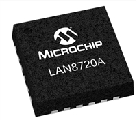
 LAN8720A的替代型号推荐、资料手册数据分析、特点介绍

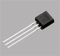
 SS8550数据手册:应用场景、主要参数分析、特性分析

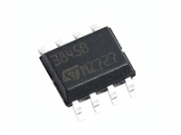
 UC3845全面解析:资料手册参数、引脚详解、维修技巧与替代型号推荐
