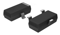
MLCC Tin/Lead Termination “B”
X8R – Specifications and Test Methods
Parameter/Test
Operating Temperature Range
Capacitance
X8R Specification Limits
-55ºC to +150ºC
Within specified tolerance
Measuring Conditions
Temperature Cycle Chamber
Freq.: 1.0 kHz ± 10%
Voltage: 1.0Vrms ± .2V
≤ 2.5% for ≥ 50V DC rating
≤ 3.5% for 25V DC and 16V DC rating
Dissipation Factor
100,000MΩ or 1000MΩ - μF,
Charge device with rated voltage for
120 ± 5 secs @ room temp/humidity
Insulation Resistance
whichever is less
Charge device with 250% of rated voltage for
1-5 seconds, w/charge and discharge current
limited to 50 mA (max)
Note: Charge device with 150% of rated voltage
for 500V devices.
Dielectric Strength
No breakdown or visual defects
Appearance
Capacitance
Variation
No defects
Deflection: 2mm
Test Time: 30 seconds
≤ ±12%
Resistance to
Flexure
Stresses
Dissipation
Factor
Meets Initial Values (As Above)
Insulation
Resistance
≥ Initial Value x 0.3
≥ 95% of each terminal should be covered
Dip device in eutectic solder at 230 ± 5ºC
for 5.0 ± 0.5 seconds
Solderability
with fresh solder
Appearance
No defects, <25% leaching of either end terminal
Capacitance
Variation
≤ ±7.5%
Dip device in eutectic solder at 260ºC for 60
seconds. Store at room temperature for 24 ± 2
hours before measuring electrical properties.
Dissipation
Factor
Insulation
Resistance
Resistance to
Solder Heat
Meets Initial Values (As Above)
Meets Initial Values (As Above)
Dielectric
Strength
Meets Initial Values (As Above)
No visual defects
≤ ±7.5%
Appearance
Step 1: -55ºC ± 2º
30 ± 3 minutes
Capacitance
Variation
Step 2: Room Temp
≤ 3 minutes
Dissipation
Factor
Meets Initial Values (As Above)
Meets Initial Values (As Above)
Step 3: +125ºC ± 2º
Step 4: Room Temp
30 ± 3 minutes
Thermal Shock
Insulation
Resistance
≤ 3 minutes
Dielectric
Strength
Appearance
Repeat for 5 cycles and measure after
24 ± 2 hours at room temperature
Meets Initial Values (As Above)
No visual defects
Capacitance
Variation
Dissipation
Factor
Insulation
Resistance
≤ ±12.5%
Charge device with 1.5 rated voltage (≤ 10V) in
test chamber set at 150ºC ± 2ºC
for 1000 hours (+48, -0)
≤ Initial Value x 2.0 (See Above)
≥ Initial Value x 0.3 (See Above)
Load Life
Remove from test chamber and stabilize at room
temperature for 24 ± 2 hours before measuring.
Dielectric
Strength
Appearance
Meets Initial Values (As Above)
No visual defects
Capacitance
Variation
Dissipation
Factor
Insulation
Resistance
Store in a test chamber set at 85ºC ± 2ºC/ 85% ±
5% relative humidity for 1000 hours
≤ ±12.5%
(+48, -0) with rated voltage applied.
≤ Initial Value x 2.0 (See Above)
≥ Initial Value x 0.3 (See Above)
Meets Initial Values (As Above)
Load
Humidity
Remove from chamber and stabilize at room
temperature and humidity for
24 ± 2 hours before measuring.
Dielectric
Strength
The Important Information/Disclaimer is incorporated in the catalog where these specifications came from or
available online at www.avx.com/disclaimer/ by reference and should be reviewed in full before placing any order.
44
112916


 共享储能电站:数据驱动与政策引领下的黄金机遇

 US1M数据手册解读:产品特性、替换型号推荐

 解析BAV99LT1G手册:参数分析、替换型号推荐

 解读BSS138PW数据手册:产品特性、电气参数及替换型号推荐
