Input/Output Functional Descriptions
Symbol
Type
Function
CK0_t, CK0_c,
CK1_t, CK1_c
Clock: CK_t and CK_c are differential clock inputs. All address and control input signals
are sampled on the crossing of the positive edge of CK_t and negative edge of CK_c.
Input
Clock Enable: CKE HIGH activates and CKE LOW deactivates internal clock signals and
device input buffers and output drivers. Taking CKE LOW provides Precharge Power-
Down and Self-Refresh operation (all banks idle), or Active Power-Down (row Active in
any bank). CKE is synchronous for Self-Refresh exit. After VREFCA and Internal DQ Vref
CKE0, CKE1
Input have become stable during the power on and initialization sequence, they must be
maintained during all operations (including Self-Refresh). CKE must be maintained high
throughout read and write accesses. Input buffers, excluding CK_t, CK_c, ODT and CKE,
are disabled during power-down. Input buffers, excluding CKE, are disabled during Self-
Refresh.
Chip Select: All commands are masked when CS_n is registered HIGH. CS_n provides for
Input external Rank selection on systems with multiple Ranks. CS_n is considered part of the
command code.
CS0_n, CS1_n,
CS2_n, CS3_n
Chip ID: Chip ID is only used for 3DS for 2 and 4 high stack via TSV to select each slice
of stacked component. Chip ID is considered part of the command code.
C0, C1
Input
On-Die Termination: ODT (registered HIGH) enables RTT_NOM termination resistance
internal to the DDR4 SDRAM. When enabled, ODT is only applied to each DQ, DQS_t,
DQS_c and DM_n/DBI_n, signal. The ODT pin will be ignored if MR1 is programmed to
ODT0, ODT1
Input
disable RTT_NOM.
Activation Command Input: ACT_n defines the Activation command being entered along
Input with CS_n. The input into RAS_n/A16, CAS_n/A15 and WE_n/A14 will be considered as
Row Address A16, A15, and A14.
ACT_n
Command Inputs: RAS_n/A16, CAS_n/A15 and WE_n/A14 (along with CS_n) define the
command being entered. Those pins have multi function. For example, for activation
Input with ACT_n Low, these are Addresses like A16, A15, and A14 but for non-activation
command with ACT_n High, these are Command pins for Read, Write, and other
command defined in command truth table.
RAS_n/A16,
CAS_n/A15,
WE_n/A14
Input Data Mask and Data Bus Inversion: DM_n is an input mask signal for write data.
Input data is masked when DM_n is sampled LOW coincident with that input data during
Input/ a Write access. DM_n is sampled on both edges of DQS. DM is muxed with DBI function.
Output DBI_n is an input/output identifying wherther to store/output the true or inverted data.
If DBI_n is LOW, the data will be stored/output after inversion inside the DDR4 SDRAM
and not inverted if DBI_n is HIGH.
DM_n/DBI_n
BG0-BG1
Bank Group Inputs: BG0 - BG1 define which bank group an Active, Read, Write, or
Precharge command is being applied. BG0 also determines which mode register is to be
accessed during a MRS cycle. For x4/8 based SDRAMs, BG0 and BG1 are valid. For x16
Input
based SDRAM components, only BG0 is valid.
Bank Address Inputs: BA0 - BA1 define to which bank an Active, Read, Write, or
Input Precharge command is being applied. Bank address also determines which mode
register is to be accessed during a MRS cycle.
BA0-BA1
Rev. 1.3 / Jan.2020
6


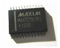
 MAX7219驱动8段数码管详解及数据手册关键信息

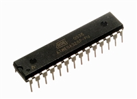
 ATMEGA328P技术资料深入分析

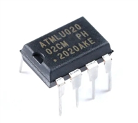
 AT24C02芯片手册管脚信息、参数分析、应用领域详解

 AT24C256芯片手册参数分析、引脚说明、读写程序示例
