King Billion Electronics Co., Ltd
HE84G770
駿 億 電 子 股 份 有 限 公 司
HE80004H SERIES
Pin Name I/O
LCAP1A O Charge Pump Capacitor Pin.
Description
LVL5
LVL4
LVL3
LVL2
LVL1
LGS1
P LCD Bias Voltage 5.
P LCD Bias Voltage 4
P LCD Bias Voltage 3
P LCD Bias Voltage 2
P LCD Bias Voltage 1.
I Regulator Voltage Setting
Voltage Regulator Output. VDD is regulated to generate LVREG, which is in turns pumped
to LVL5. Adjust resistor between LGS1 and LVREG to set LVREG voltage.
LVREG
O
VR12
GND
VO
I Charge Pump Input. The buffered output of the fine-adjusted VREG.
P Power Ground Input.
O DAC Output.
DAO
OPIN
OPIP
OPO
O Alternate output of DAC.
I Inverting input of OP Amp.
I Non-inverting input of OP Amp.
O Output of OP Amp.
RSTP_N
I System Reset Input Pin. Level trigger, active low on this pin will put the chip in reset state.
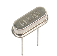
External fast clock pin. Two types of oscillator can be selected by MO_FXTAL (‘0’ for RC
O, type and ‘1’ for crystal type). For RC type oscillator, one resistor needs to be connected
B between FXI and GND. For crystal oscillator, one crystal needs to be placed between FXI
and FXO. Please refer to application for details.
FXO,
FXI
Test input pin. Please bond this pad and reserve a test point on PCB for debugging. But for
TSTP_P
I
improving ESD, please connect this point with zero Ohm resistor to GND.
External slow clock pins. Slow clock is clock source for LCD display, TIMER1, Time-Base
O, and other internal blocks. Both crystal and RC oscillator are provided. The slow clock type
I can be selected by mask option MO_SXTAL. Choose ‘0’ for RC type and ‘1’ for crystal
oscillator.
SXO,
SXI
Input pin for x32 PLL circuit. Connect to external resistor and capacitors as shown in
VX
I
application circuit.
OLFR
OCCK
O LCD frame signal for interfacing with LCD segment extender KDGS80.
O LCD data load pin for interfacing with LCD segment extender KDGS80.
Positive power Input. A 0.1 µF decoupling capacitors should be placed as close to IC VDD
VDD
P
and GND pads as possible for best decoupling effect.
8-bit bi-directional I/O port D. The output type of I/O pad can also be selected by mask
option MO_DPP[7..0] (‘1’ for push-pull and ‘0’ for open-drain).
As the output structure of I/O pad does not contain tri-state buffer. When using the I/O as
B input, ‘1’ must be outputted before reading the pin.
PRTD[7..2]
PRTD[1]/SIN
PRTD[0]/SOUT
PRTD[7..2] can be used as wake-up pins. PRTD[7..6] can be as external interrupt sources.
PRTD[1] shares pad with UART Receiver SIN pin.
PRTD[0] shares pad with UART transmitter SOUT pin.
O Dedicated Ground for PWM output.
GND_PWM
PWM
The PWM output can drive speaker or buzzer directly. Set the bit2 of VOC register as one to
O
turn on PWM. Using VDD & PWM to drive output device.
IRO
O The Infrared output.
4-bit bi-directional I/O port C. The output type of I/O pad can also be selected by mask
option MO_CPP[7..4] (‘1’ for push-pull and ‘0’ for open-drain).
PRTC[7..4]/
SCNI[3..0]
As the output structure of I/O pad does not contain tri-state buffer. When using the I/O as
B
input, ‘1’ must be outputted before reading the pin.
PRTC[7..4] is shared with Key Scan Dedicated Input SCNI[3..0]. The Key Scan function
can be disabled by clearing MO_LCDKEY mask option to ‘0’.
P Dedicated power input for RAM
VDD_RAM
CMSG[32..79] O COM[32..79] pads are shared with SEG[127..80] outputs. The functions of the pads to be
October 31, 2003
5
Version:V1.1
This specification is subject to change without notice. Please contact sales person for the latest version before use.


 资料手册解读:UC3842参数和管脚说明

 一文带你了解无源晶振的负载电容为何要加两颗谐振电容CL1和CL2

 玻璃管保险丝与陶瓷管保险丝:区别与替代性探讨

 PCF8574资料解读:主要参数分析、引脚说明
