
 5秒后页面跳转

| 型号 | 品牌 | 获取价格 | 描述 | 数据表 |
| GS81302R37GE-400IT | GSI |
获取价格 |
DDR SRAM, 4MX36, 0.45ns, CMOS, PBGA165, 15 X 17 MM, 1 MM PITCH, ROHS COMPLIANT, FBGA-165 |

|
| GS81302S08 | GSI |
获取价格 |
144Mb SigmaSIOTM DDR -II Burst of 2 SRAM |
|
| GS81302S08E-167IT | GSI |
获取价格 |
DDR SRAM, 8MX8, 0.5ns, CMOS, PBGA165, 17 X 15 MM, 1 MM PITCH, FPBGA-165 |
|
| GS81302S08E-200I | GSI |
获取价格 |
DDR SRAM, 8MX8, 0.45ns, CMOS, PBGA165, 17 X 15 MM, 1 MM PITCH, FPBGA-165 |
|
| GS81302S08E-200IT | GSI |
获取价格 |
DDR SRAM, 8MX8, 0.45ns, CMOS, PBGA165, 17 X 15 MM, 1 MM PITCH, FPBGA-165 |
|
| GS81302S08E-250 | GSI |
获取价格 |
165 BGA |
|
| GS81302S08E-250I | GSI |
获取价格 |
165 BGA |
|
| GS81302S08E-250IT | GSI |
获取价格 |
DDR SRAM, 16MX8, 0.45ns, CMOS, PBGA165, 15 X 17 MM, 1 MM PITCH, MO-216CAB-1, FPBGA-165 |
|
| GS81302S08E-250T | GSI |
获取价格 |
DDR SRAM, 16MX8, 0.45ns, CMOS, PBGA165, 15 X 17 MM, 1 MM PITCH, MO-216CAB-1, FPBGA-165 |
|
| GS81302S08E-300 | GSI |
获取价格 |
165 BGA |
|
 MAX232IDR数据手册:产品特性、电气参数、替代型号推荐

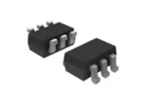 2N7002DW数据手册:参数解读、引脚信息、替代型号推荐
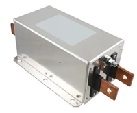 网络滤波器、EMI滤波器与EMC滤波器在电子元器件中的分类关系
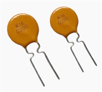 NTC热敏电阻与PTC热敏电阻的应用原理及选型原则
工作时间:9:00-21:00
CEO邮箱:ceo@jiepei.com
投诉邮箱:tousu@jiepei.com


 浙公网安备 33010502006866号 浙ICP备10014259号-119
营业执照ICP证
浙公网安备 33010502006866号 浙ICP备10014259号-119
营业执照ICP证


