93LC46/56/57/66/86
The format for all instructions sent to the device is a
logical"1"startbit,a2-bit(or4-bit)opcode,6-bit(93LC46)/
increment to the next address and shift out the next data
word in a sequential READ mode. As long as CS is
/7-bit (93LC57)/ 8-bit (93LC56 or 93LC66)/10-bit (93LC86) continuously asserted and SK continues to toggle, the
(an additional bit when organized X8) and for write
operationsa16-bitdatafield(8-bitforX8organizations).
device will keep incrementing to the next address
automatically until it reaches to the end of the address
space, then loops back to address 0. In the sequential
READ mode, only the initial data word is preceeded by
a dummy zero bit. All subsequent data words will follow
without a dummy zero bit.
Note: This note is applicable only to 93LC86. The Write,
Erase, Write all and Erase all instructions require PE=1.
If PE is left floating, 93C86 is in Program Enabled mode.
ForWriteEnableandWriteDisableinstructionPE=don’t
care.
Write
Read
After receiving a WRITE command, address and the
data, the CS (Chip Select) pin must be deselected for a
minimum of tCSMIN. The falling edge of CS will start the
self clocking clear and data store cycle of the memory
location specified in the instruction. The clocking of the
SK pin is not necessary after the device has entered the
self clocking mode. The ready/busy status of the
93LC46/56/57/66/86canbedeterminedbyselecting
the device and polling the DO pin. Since this device
features Auto-Clear before write, it is NOT necessary to
erase a memory location before it is written into.
Upon receiving a READ command and an address
(clocked into the DI pin), the DO pin of the 93LC46/
56/57/66/86 will come out of the high impedance state
and, after sending an initial dummy zero bit, will begin
shifting out the data addressed (MSB first). The output
databitswilltoggleontherisingedgeoftheSKclockand
are stable after the specified time delay (tPD0 or tPD1).
For the 93LC56/57/66/86, after the initial data word
has been shifted out and CS remains asserted with the
SKclockcontinuingtotoggle,thedevicewillautomatically
Figure 2b. Read Instruction Timing (93LC56/57/66/86)
SK
1
1
1
1
1
1
1
1
1
1
1
1
1
1
1
CS
DI
Don't Care
A
A
A
0
N
N–1
1
1
0
HIGH-Z
DO
Dummy 0
D
D
Address + 1 Address + 2 Address + n
15 . . .
0
or
D
D
D
D
D
15 . . .
0
15 . . .
0
15 . . .
D
D
or
or
or
7 . . .
0
D
D
D
D
D
7 . . .
7 . . .
0
7 . . .
0
Figure 3. Write Instruction Timing
SK
t
CSMIN
STANDBY
STATUS
VERIFY
CS
A
A
A
0
D
D
0
N
N-1
N
DI
1
0
1
t
t
SV
HZ
BUSY
HIGH-Z
DO
READY
HIGH-Z
t
EW
93LC46/56/57/66/86 F05
Doc. No. 1023, Rev. G
7


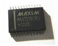
 MAX7219驱动8段数码管详解及数据手册关键信息

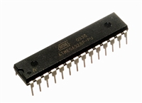
 ATMEGA328P技术资料深入分析

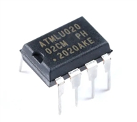
 AT24C02芯片手册管脚信息、参数分析、应用领域详解

 AT24C256芯片手册参数分析、引脚说明、读写程序示例
