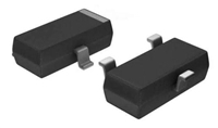
Crystal oscillator
Epson Toyocom
Product Number (please contact us)
EG-2121CA: Q3805CAx0xxxx00
EG-2102CA: Q3806CA00xxxx00
CRYSTAL OSCILLATOR
LOW-JITTER SAW OSCILLATOR
EG-2121
/
2102CA series
•Frequency range
•Supply voltage
:
:
:
:
:
53.125 MHz to 700 MHz
2.5 V (EG-2121CA)
3.3 V (EG-2102CA)
Differential LV-PECL or LVDS
Output enable(OE)
•Output
•Function
•External dimensions : 7.0 × 5.0 × 1.2 t (mm) Typ.
•Very low jitter and low phase noise by SAW unit.
Actual size
EG-2102CA
EG-2121CA
Specifications (characteristics)
EG-2121CA
EG-2102CA
EG-2121CA
EG-2102CA
LVDS
Item
Symbol
Remarks
Differential LV-PECL
53.125 MHz to
500 MHz
2.5 V ±0.125 V
100 MHz to
700 MHz
3.3 V ±0.3 V
Please contact us for inquiries regarding available
frequencies.
Output frequency range
Supply voltage
53.125 MHz to 700 MHz
2.5 V ±0.125 V 3.3 V ±0.3 V
f
0
VCC
Storage temperature
Operating temperature
-40 °C to +100 °C
P:0 °C to +70 °C ,R:-5 °C to +85 °C ,S:-20 °C to +70 °C
G: ± 50 × 10-6 ,H: ±100 × 10-6
Store as bare product after unpacking
T_stg
T_use
Temperature
range
Please contact us for inquiries about S spec.
P:0 °C to +70 °C,R:-5 °C to +85 °C *1
,S:-20 °C to +70 °C
Frequency tolerance
f_tol
Current consumption
Disable current
Symmetry
ICC
I_dis
SYM
80 mA Max.
20 mA Max.
100 mA Max.
32 mA Max
30 mA Max
20 mA Max
45 mA Max.
30 mA Max.
OE=VCC,RL=50 Ω or 100 Ω
OE=GND
P:45 % to 55 % P:45 % to 55 % L:45 % to 55 % L:45 % to 55 % f0≤350 MHz (at outputs crossing point) *1
1.55 V Typ. 2.35 V Typ.
VCC-1.025 V to VCC-0.88 V
0.8 V Typ. 1.6 V Typ.
VOH
DC characteristics
VOL
VCC-1.81 V to VCC-1.62 V
Output voltage
Differential output, DC characteristics
Output change, DC characteristics
Offset, DC characteristics
VOD
∆VOD
VOS
350 mV Typ. 247 mV to 454 mV
50 mV
1.25 V Typ. 1.125 V to 1.375 V
150 mV
Offset change, DC characteristics
LV-PECL: Terminated to VCC -2.0 V
∆VOS
Output load condition
RL
50 Ω
100 Ω
LVDS: Connected between OUT to OUT
OE terminal
Output enable input voltage
Output disable input voltage
VIH
VIL
70 % VCC Min.
30 % VCC Max.
OE terminal
Between 20% VCC and80%of (VOH-VOL)
Between 20 %and 80 %of Differential
Output peek to peek voltage
Rise time / Fall time
Start-up time
t
r / t
f
400 ps Max.
Time at minimum supply voltage to be 0 s
t_str
10 ms Max.
0.2 ps Typ.
3 ps Typ.
3 ps Typ.
25 ps Typ.
Deterministic Jitter
t
DJ
RJ
Random Jitter
t
Jitter *2
t
RMS
σ (RMS of total distribution)
Peak to Peak
tp-p
acc
t
4 ps Typ.
Accumulated Jitter(σ) n=2 to 50000 cycles
0.05 × 10⁻³ UI Typ.
1 ps Max.
Phase Jitter
tPJ
Offset frequency: 12 kHz to 20 MHz
Frequency aging *3
*1 As per below table.
f_aging
± 10 × 10-6 / year Max.
+25 °C,First year,VCC=2.5 V,3.3 V
*2 Based on DTS-2075 Digital timing system made from WAVECREST with jitter analysis software VISI6.
*3 Except: ***A
Output mode
Frequency
range
P:Differential LV-PECL
All range
D: Differential LV-PECL
L:LVDS
V:LVDS
EG-2121CA
EG-2102CA
f
0 ≤ 175 MHz
0 ≤ 350 MHz
All range
f
0 ≤ 175 MHz
f
50 ± 10 %(f
50 ± 5 %(f00≤>335500MMHHzz))
50 ± 2 %
50 ± 2 %
EG-2121CA
EG-2102CA
50 ± 10 %(f0 > 350 MHz)
50 ± 5 %(f0 ≤ 350 MHz)
Symmetry
50 ± 5 %
Details of frequency tolerance
A *4
PHPA
PHRA*6
PGPA*6
N *5
PHPN
PHRN*6
PGPN*6
PGRN*6
A *4
DHPA
DHRA*6
DGPA*6
N *5
DHPN
DHRN*6
DGPN*6
DGRN*6
A *4
LHPA
LHRA*6
LGPA*6
N *5
LHPN
LHRN*6
LGPN*6
LGRN*6
A *4
VHPA
VHRA*6
VGPA*6
N *5
VHPN
VHRN*6
VGPN*6
VGRN*6
HP: ±100 × 10-6(0°C to +70°C)
Frequency
tolerance
HR: ±100 × 10-6(-5°C to +85°C)
GP: ±50 × 10-6(0°C to +70°C)
GR: ±50 × 10-6(-5°C to +85°C)
*4 This includes initial frequency tolerance, temperature variation, supply voltage variation, reflow drift, and aging(+25 °C,10 years).
*5 This includes initial frequency tolerance, temperature variation, supply voltage variation, and reflow drift(except aging).
*6 53.125 MHz ≤ f0 < 100 MHz : Unavailable.
External dimensions
(Unit:mm)
Footprint (Recommended)
(Unit:mm)
1.6
1.4
#6
#5
#4
#4
#5
#6
#1
Pin map
Pin
Connection
OE
N.C.
GND
OUT
OUT
E EG-2121
250.000P
GPA 282A
1
2
3
4
5
6
#2
7.0±0.2
#3
#1
VCC
#3
#2
5.08
2.54
2.54
5.08
#3 is connected to the cover.
To maintain stable operation, provide by-pass capacitor with
more than 0.1 μF at a location as near as possible to the power
source terminal of the crystal products (between VCC - GND).
5.08
http://www.epsontoyocom.co.jp


 共享储能电站:数据驱动与政策引领下的黄金机遇

 US1M数据手册解读:产品特性、替换型号推荐

 解析BAV99LT1G手册:参数分析、替换型号推荐

 解读BSS138PW数据手册:产品特性、电气参数及替换型号推荐
