
| 是否Rohs认证: | 符合 | 生命周期: | Obsolete |
| 零件包装代码: | SOIC | 包装说明: | SOP, SOP14,.25 |
| 针数: | 14 | Reach Compliance Code: | unknown |
| HTS代码: | 8542.39.00.01 | 风险等级: | 5.03 |
| 系列: | 4000/14000/40000 | JESD-30 代码: | R-PDSO-G14 |
| JESD-609代码: | e3 | 长度: | 8.65 mm |
| 负载电容(CL): | 50 pF | 逻辑集成电路类型: | D FLIP-FLOP |
| 最大频率@ Nom-Sup: | 2500000 Hz | 湿度敏感等级: | 1 |
| 位数: | 1 | 功能数量: | 2 |
| 端子数量: | 14 | 最高工作温度: | 125 °C |
| 最低工作温度: | -55 °C | 输出极性: | COMPLEMENTARY |
| 封装主体材料: | PLASTIC/EPOXY | 封装代码: | SOP |
| 封装等效代码: | SOP14,.25 | 封装形状: | RECTANGULAR |
| 封装形式: | SMALL OUTLINE | 包装方法: | TAPE AND REEL |
| 峰值回流温度(摄氏度): | 260 | 电源: | 5/15 V |
| Prop。Delay @ Nom-Sup: | 350 ns | 传播延迟(tpd): | 350 ns |
| 认证状态: | Not Qualified | 座面最大高度: | 1.75 mm |
| 子类别: | FF/Latches | 最大供电电压 (Vsup): | 15 V |
| 最小供电电压 (Vsup): | 3 V | 标称供电电压 (Vsup): | 5 V |
| 表面贴装: | YES | 技术: | CMOS |
| 温度等级: | MILITARY | 端子面层: | Matte Tin (Sn) |
| 端子形式: | GULL WING | 端子节距: | 1.27 mm |
| 端子位置: | DUAL | 处于峰值回流温度下的最长时间: | NOT SPECIFIED |
| 触发器类型: | POSITIVE EDGE | 宽度: | 3.9 mm |
| 最小 fmax: | 7.6 MHz | Base Number Matches: | 1 |
| 型号 | 品牌 | 替代类型 | 描述 | 数据表 |
| CD4013BCM | FAIRCHILD |
类似代替  |
Dual D-Type Flip-Flop |

|
| MC14013BDR2G | ONSEMI |
功能相似 |
Dual Type D Flip−Flop |
|
| MC14013BDTR2G | ONSEMI |
功能相似 |
Dual Type D Flip−Flop |
|
| 型号 | 品牌 | 获取价格 | 描述 | 数据表 |
| CD4013BCMX_NL | FAIRCHILD |
获取价格 |
D Flip-Flop, 4000/14000/40000 Series, 2-Func, Positive Edge Triggered, 1-Bit, Complementar |
|
| CD4013BCM_NL | FAIRCHILD |
获取价格 |
D Flip-Flop, 4000/14000/40000 Series, 2-Func, Positive Edge Triggered, 1-Bit, Complementar |
|
| CD4013BCN | FAIRCHILD |
获取价格 |
Dual D-Type Flip-Flop |
|
| CD4013BCN | NSC |
获取价格 |
Dual D Flip-Flop |
|
| CD4013BCN | ONSEMI |
获取价格 |
类型:D 型;功能模块数:2;最大工作频率(MHz):15.5 MHz;支持工作位数:1; |
|
| CD4013BCN/A+ | TI |
获取价格 |
IC,FLIP-FLOP,DUAL,D TYPE,CMOS,DIP,14PIN,PLASTIC |
|
| CD4013BCN/B+ | TI |
获取价格 |
IC,FLIP-FLOP,DUAL,D TYPE,CMOS,DIP,14PIN,PLASTIC |
|
| CD4013BCSJ | FAIRCHILD |
获取价格 |
Dual D-Type Flip-Flop |
|
| CD4013BCSJX | FAIRCHILD |
获取价格 |
Dual D-Type Flip-Flop |
|
| CD4013BCSJX | ONSEMI |
获取价格 |
类型:D 型;功能模块数:2;最大工作频率(MHz):15.5 MHz;支持工作位数:1; |
|
 Intel 未来两代 Core 处理器深度解析:Panthe、Nova

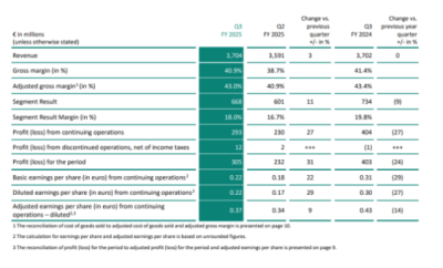 英飞凌2025年第三季度财报出炉:营收同比增长3% 利润率显著提升
 英伟达回应:芯片不存在后门、终止开关与监控软件
 105亿!Amphenol史上最大收购震撼业界
工作时间:9:00-21:00
CEO邮箱:ceo@jiepei.com
投诉邮箱:tousu@jiepei.com


 浙公网安备 33010502006866号 浙ICP备10014259号-119
营业执照ICP证
浙公网安备 33010502006866号 浙ICP备10014259号-119
营业执照ICP证


