AS29F010
AS29F011
MODE TABLE
†
Mode
RP
CE
OE
WE
A0
A9
I/O
HI-Z
Deep power down
Read
L
X
L
L
H
L
L
L
X
L
X
H
H
H
H
H
L
X
X
H
H
H
H
H
H
A0
X
A9
X
D
OUT
Output disable
Standby
H
H
L
HI-Z
HI-Z
52h
X
X
Mfr. code
L
Vh
Vh
A9
Part code
L
H
03h
Write command
H
A0
D
IN
†
RP is used only on the AS29F011. Key: L =Low (<V ); H = High (>V ); Vh = 11.5–12.5V; X =Don’t care
IL
IH
Deep power down: (AS29F011 only): RP low; all DC power
disabled. This interrupts any command in progress.
CE and OE are pulled low the outputs are enabled and a data byte
is read out. When A0 is pulled low the output data = 52h, a unique
Mfr. code for Alliance Semiconductor Flash products. When A0 is
Read mode: Selected with CE and OE low, WE high. Data is valid
high D
= 03h, the Alliance part code for the AS29F010.
OUT
T
after addresses are stable, T after CE is low and T after
aa
CE OE
OE is low.
Write command: Selected by CE and WE pulled low, OE pulled
high. Initiates command mode in the WSM and latches addresses
and data into the chip. Once a write command starts, the WSM
stays in command mode until the command is completed or it
times out. Addresses are latched on the falling edge of WE and
CE; data is latched on the rising edge. The WE signal is filtered to
prevent spurious events from being detected as write commands.
Output disable: Part remains powered up; but outputs disabled
with OE pulled high.
Standby: Part is powered down, and I reduced to 1.5 mA for
TTL input levels (<1.0 mA for CMOS input levels).
CC
Mfr. (manufacturer) code, Part code: Selected by A9 = 11.5–
12.5V per the JEDEC standard for non-volatile memories. When
COMMAND FORMAT
All commands require four bus write cycles to execute. After four
write cycles the command executes until terminated by the internal
command sequence to execute. The AS29F010 does not remain in
command mode after time-out. When a command times-out only
the error flag is not reset.
timer. For verify commands a read operation after Write in a
[4]
write command bus cycle reads out the data from the array. For
manufacturer and part code commands the ID code is read out. For
other operations a read operation reads out a status byte on the
outputs.
Errors and timeout: Any of the following conditions sets the
error flag.
•
•
•
•
Any write command which does not match the sequence
above for Write . Write , and Write
.
[3]
{1]
{2]
ADDRESS IN
DATA IN
Any write cycle that follows more than 150 µs after the
previous write cycle.
Bus Write
Bus Write
Bus Write
Bus Write
Bus read
5555h
AAh
[1]
[2]
[3]
[4]
2AAAh
5555h
55h
The command Data in Write has more than one bit set
[3]
[3]
Command code
Data in
high. This indicates conflicting commands.
Address in
Address in
V
drops below V during command execution.
D
CC
LKO
OUT
Once the error flag is set, the AS29F010 times out and returns to
normal mode. The error flag remains until it is cleared by a reset
command. The error flag can be read by executing a status
command and reading the status byte.
Command timeout: For each operation the address and data are
latched at bus Write and held until the operation completes and
[4]
times-out. After time-out the WSM returns the AS29F010 to
normal mode. Each individual operation requires the 4-cycle write
3


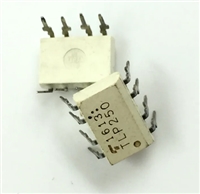
 TLP250光耦合器:资料手册参数分析

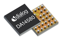
 DA14580 低功耗蓝牙系统级芯片(SoC):资料手册参数分析

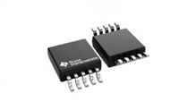
 INA226 高精度电流和功率监控器:资料手册参数分析

 SI2302 N沟道MOSFET:资料手册参数分析
