
 5秒后页面跳转

| 是否Rohs认证: | 不符合 | 生命周期: | Contact Manufacturer |
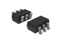
| 零件包装代码: | SOIC | 包装说明: | SOIC-24 |
| 针数: | 24 | Reach Compliance Code: | unknown |
| ECCN代码: | EAR99 | HTS代码: | 8542.33.00.01 |
| 风险等级: | 5.7 | Is Samacsys: | N |
| 放大器类型: | OPERATIONAL AMPLIFIER | 最大平均偏置电流 (IIB): | 0.0002 µA |
| 标称共模抑制比: | 83 dB | 最大输入失调电压: | 11000 µV |
| JESD-30 代码: | R-PDSO-G24 | 湿度敏感等级: | 1 |
| 标称负供电电压 (Vsup): | -2.5 V | 功能数量: | 4 |
| 端子数量: | 24 | 最高工作温度: | 70 °C |
| 最低工作温度: | 封装主体材料: | PLASTIC/EPOXY | |
| 封装形状: | RECTANGULAR | 封装形式: | SMALL OUTLINE |
| 峰值回流温度(摄氏度): | 225 | 认证状态: | Not Qualified |
| 标称压摆率: | 0.17 V/us | 最大压摆率: | 0.2 mA |
| 标称供电电压 (Vsup): | 2.5 V | 表面贴装: | YES |
| 技术: | CMOS | 温度等级: | COMMERCIAL |
| 端子形式: | GULL WING | 端子位置: | DUAL |
| 处于峰值回流温度下的最长时间: | NOT SPECIFIED | 标称均一增益带宽: | 200 kHz |
| Base Number Matches: | 1 |
| 型号 | 品牌 | 获取价格 | 描述 | 数据表 |
| ALD4706BSB | ALD |
获取价格 |
Operational Amplifier |

|
| ALD4706BSBL | ALD |
获取价格 |
DUAL ULTRA MICROPOWER RAIL-TO-RAIL CMOS OPERATIONAL AMPLIFIER |
|
| ALD4706BSF | ETC |
获取价格 |
Analog IC |
|
| ALD4706DB | ALD |
获取价格 |
Operational Amplifier |
|
| ALD4706PB | ALD |
获取价格 |
Operational Amplifier |
|
| ALD4706PBL | ALD |
获取价格 |
DUAL ULTRA MICROPOWER RAIL-TO-RAIL CMOS OPERATIONAL AMPLIFIER |
|
| ALD4706SB | ALD |
获取价格 |
Operational Amplifier |
|
| ALD4706SBL | ALD |
获取价格 |
DUAL ULTRA MICROPOWER RAIL-TO-RAIL CMOS OPERATIONAL AMPLIFIER |
|
| ALD4706SF | ETC |
获取价格 |
Analog IC |
|
| ALD500 | ALD |
获取价格 |
PRECISION INTEGRATING ANALOG PROCESSOR |
|
 MAX232IDR数据手册:产品特性、电气参数、替代型号推荐

 2N7002DW数据手册:参数解读、引脚信息、替代型号推荐
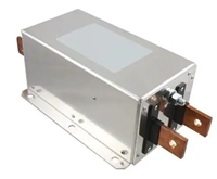 网络滤波器、EMI滤波器与EMC滤波器在电子元器件中的分类关系
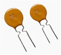 NTC热敏电阻与PTC热敏电阻的应用原理及选型原则
工作时间:9:00-21:00
CEO邮箱:ceo@jiepei.com
投诉邮箱:tousu@jiepei.com


 浙公网安备 33010502006866号 浙ICP备10014259号-119
营业执照ICP证
浙公网安备 33010502006866号 浙ICP备10014259号-119
营业执照ICP证


