AD6623
Bit 6
Can be set through the serial port (see section on
serial word formats).
(0xn17) Power Ramp Length 0
This is the length of the ramp for mode 0, minus one.
Bits 3–0: Sets (NRCF/LRCF) –1
(0xn18) Power Ramp Length 1
This is the length of the ramp for mode 1, minus one. Setting
this to zero disables dual ramps.
(0xn0D) Channel Mode Control 2
Bits 7–6: Sets the RCF Coarse Scale as shown in Table XXIII.
(0xn19) Power Ramp Rest Time
Table XXIII. RCF Coarse Scale
This is the number of RCF output samples to rest for between a
ramp down and a ramp up.
Bit 7
Bit 6
RCF Coarse Scale (dB)
(0xn1A–0xn1F) Unused
0
0
1
1
0
1
0
1
0
–6
–12
–18
(0xn20–0xn3F) Data Memory
This group of registers contain the RCF Filter Data. See the RCF
section for additional details.
(0xn40–0xn17F) Power Ramp Coefficient Memory
This group of registers contain the Power Ramp Coefficients.
See the Power Ramp section for additional details.
Bit 5:
High enables the RCF phase equalizer.
Bits 4–0: Sets the serial clock divider (SDIV) that determines the
serial clock frequency based on the following equation.
(0xn80–0xn1FF) Coefficient Memory
This group of registers contain the RCF Filter Coefficients.
See the RCF section for additional details.
CLK
SDIV +1
fSCLK
=
(28)
(0xn0E) Fine Scale Factor
PSEUDOCODE
Bits 15–2: Sets the RCF Fine Scale Factor as an unsigned number
representing the values (0,2). This register is shad-
owed for synchronization purposes. The shadow can
be read back directly, the Fine Scale Factor can not.
Bits 1–0: Reserved.
Write Pseudocode
Void Write_Micro(ext_address, int data);
Main()
{
/* This code shows the programming of the
NCO frequency register using the Write_Micro
function defined above. The variable
address is the External Address A[2:0] and
data is the value to be placed in the
external interface register.
(0xn0F) RCF Time Slot Hold-Off Counter
Bits 17–16: The Time Slot Sync Select bits are used to set which
sync pin will initiate a time slot sync sequence.
Bits 15–0: The Hold-Off Counter is used to synchronize the
change of RCF Fine Scale. See the Synchronization
section for a detailed explanation. If no synchroniza-
tion is required, this register should be set to 0.
Internal Address = 0x102, channel 1
*/
(0xn10–0xn11) RCF Phase Equalizer Coefficients
See the RCF section for details.
/*Holding registers for NCO byte wide
access data*/
(0xn12–0xn15) FIR-PSK Magnitudes
See the RCF section for details.
int d3, d2, d1, d0;
/*NCO frequency word (32 bits wide)*/
NCO_FREQ=0x1BEFEFFF;
/*write Chan */
Write_Micro(7, 0x01);
/*write Addr */
Write_Micro(6,0x02);
/*write Byte 3*/
(0xn16) Serial Port Setup
Bits 7–6: Serial Data Frame Start Select
Title XXIV. Serial Port Setup
Bit 7
Bit 6
Serial Data Frame Start
d3=(NCO_FREQ & 0xFF02Y∞00)>>24;
Write_Micro(3,d3);
0
1
1
X
0
1
Internal Frame Request
External SDFI Pad
Previous Channel’s Frame End
/*write Byte 2*/
d2=(NCO_FREQ & 0xFF0000)>>16;
Write_Micro(2,d2);
/*write Byte 1*/
d1=(NCO_FREQ & 0xFF00)>>8;
Write_Micro(1,d1);
/*write Byte 0, Byte 0 is written last and
causes an internal write to occur*/
d0=NCO_FREQ & 0xFF;
Write_Micro(0,d0);
}
Bit 5:
Bit 4:
Bit 3:
Bit 2:
High means SDFO is a frame end, low means SDFO
is a frame request.
High selects serial slave mode. SCLK is an input in
serial slave mode.
High enables Fine Scaling through the Serial Port
(not available in FIR Mode).
High enables Serial Time Slot Syncs (not available
in FIR Mode).
Bit 1:
Bit 0:
High enables Power Ramp coefficient interpolation.
High enables the Power Ramp.
REV. 0
–35–


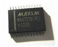
 MAX7219驱动8段数码管详解及数据手册关键信息

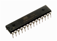
 ATMEGA328P技术资料深入分析

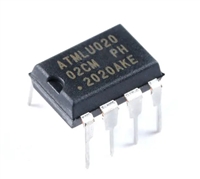
 AT24C02芯片手册管脚信息、参数分析、应用领域详解

 AT24C256芯片手册参数分析、引脚说明、读写程序示例
