
| 型号 | 品牌 | 获取价格 | 描述 | 数据表 |
| 74LVC2T45 | NXP |
获取价格 |
Dual supply translating transceiver; 3-state |

|
| 74LVC2T45 | SGMICRO |
获取价格 |
2-Bit Dual-Supply Bus Transceiver with Configurable Voltage Translation |
|
| 74LVC2T45 | DIODES |
获取价格 |
Dual Bit Voltage Translator |
|
| 74LVC2T45-Q100 | NEXPERIA |
获取价格 |
Dual supply translating transceiver; 3-state |
|
| 74LVC2T45DC | NXP |
获取价格 |
Dual supply translating transceiver; 3-state |
|
| 74LVC2T45DC | NEXPERIA |
获取价格 |
Dual supply translating transceiver; 3-stateProduction |
|
| 74LVC2T45DC,125 | NXP |
获取价格 |
74LVC2T45; 74LVCH2T45 - Dual supply translating transceiver; 3-state SSOP 8-Pin |
|
| 74LVC2T45DC,125 | NEXPERIA |
获取价格 |
输出电压类型:三态,非反相 ;单电路的通道数(channel):2 ;VCCA最小值(V) |
|
| 74LVC2T45DC-Q100 | NEXPERIA |
获取价格 |
Dual supply translating transceiver; 3-state |
|
| 74LVC2T45DC-Q100H | NEXPERIA |
获取价格 |
输出电压类型:三态,非反相;单电路的通道数(channel):2;通道方向类型:双向;元器 |
|
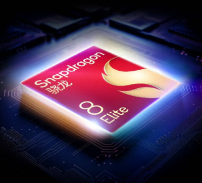 高通第五代骁龙8至尊版发布:能效提升30%的移动芯片革命

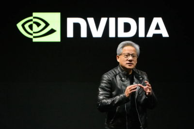 阿里巴巴联手英伟达进军Physical AI 中国AI技术迎来关键突破
 微软突破性微流控技术:AI芯片降温65%或将重塑数据中心未来
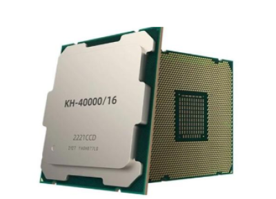 国产x86处理器里程碑!兆芯6000台医疗电脑中标某总医院
工作时间:9:00-21:00
CEO邮箱:ceo@jiepei.com
投诉邮箱:tousu@jiepei.com


 浙公网安备 33010502006866号 浙ICP备10014259号-119
营业执照ICP证
浙公网安备 33010502006866号 浙ICP备10014259号-119
营业执照ICP证


