
 5秒后页面跳转

| 型号 | 品牌 | 替代类型 | 描述 | 数据表 |
| 74HC299PW,118 | NXP |
完全替代  |
74HC299 - 8-bit universal shift register; 3-state@en-us TSSOP2 20-Pin |

|
| 74HC299PW | NXP |
功能相似 |
8-bit universal shift register; 3-state |
|
| 型号 | 品牌 | 获取价格 | 描述 | 数据表 |
| 74HC299PW,118 | NXP |
获取价格 |
74HC299 - 8-bit universal shift register; 3-state@en-us TSSOP2 20-Pin |
|
| 74HC299PW-T | NXP |
获取价格 |
IC HC/UH SERIES, 8-BIT BIDIRECTIONAL PARALLEL IN PARALLEL OUT SHIFT REGISTER, TRUE OUTPUT, |
|
| 74HC2G00 | NXP |
获取价格 |
Dual 2-input NAND gate |
|
| 74HC2G00DC | NEXPERIA |
获取价格 |
Dual 2-input NAND gateProduction |
|
| 74HC2G00DC | NXP |
获取价格 |
Dual 2-input NAND gate |
|
| 74HC2G00DC-G | NXP |
获取价格 |
暂无描述 |
|
| 74HC2G00DC-Q100 | NXP |
获取价格 |
IC NAND GATE, Gate |
|
| 74HC2G00DC-Q100 | NEXPERIA |
获取价格 |
Dual 2-input NAND gateProduction |
|
| 74HC2G00DP | NXP |
获取价格 |
Dual 2-input NAND gate |
|
| 74HC2G00DP | NEXPERIA |
获取价格 |
Dual 2-input NAND gateProduction |
|
 DS1135-8资料手册解读:深入探索高速硅定时电路的特性与应用

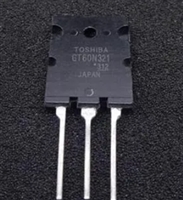 GT60N321资料手册解读:深入了解东芝第四代绝缘栅双极晶体管
 STS5DNE30L资料手册解读:参数分析、特性与应用
 MDU1511资料手册解读:探索这款MOSFET的全面特性
工作时间:9:00-21:00
CEO邮箱:ceo@jiepei.com
投诉邮箱:tousu@jiepei.com


 浙公网安备 33010502006866号 浙ICP备10014259号-119
营业执照ICP证
浙公网安备 33010502006866号 浙ICP备10014259号-119
营业执照ICP证


