512 Kbit / 1 Mbit / 2 Mbit / 4 Mbit (x8) Multi-Purpose Flash
SST39LF512 / SST39LF010 / SST39LF020 / SST39LF040
SST39VF512 / SST39VF010 / SST39VF020 / SST39VF040
SST39LF/VF512 / 010 / 020 / 0403.0 & 2.7V 512Kb / 1Mb / 2Mb / 4Mb (x8) MPF memories
Data Sheet
FEATURES:
•
•
Organized as 64K x8 / 128K x8 / 256K x8 / 512K x8
Single Voltage Read and Write Operations
•
Fast Erase and Byte-Program:
– Sector-Erase Time: 18 ms (typical)
– Chip-Erase Time: 70 ms (typical)
– Byte-Program Time: 14 µs (typical)
– Chip Rewrite Time:
– 3.0-3.6V for SST39LF512/010/020/040
– 2.7-3.6V for SST39VF512/010/020/040
•
•
Superior Reliability
1 second (typical) for SST39LF/VF512
2 seconds (typical) for SST39LF/VF010
4 seconds (typical) for SST39LF/VF020
8 seconds (typical) for SST39LF/VF040
– Endurance: 100,000 Cycles (typical)
– Greater than 100 years Data Retention
Low Power Consumption:
•
•
Automatic Write Timing
– Internal VPP Generation
End-of-Write Detection
– Active Current: 10 mA (typical)
– Standby Current: 1 µA (typical)
•
•
Sector-Erase Capability
– Uniform 4 KByte sectors
Fast Read Access Time:
– Toggle Bit
– Data# Polling
•
•
CMOS I/O Compatibility
JEDEC Standard
– 45 ns for SST39LF512/010/020/040
– 55 ns for SST39LF020/040
– 70 and 90 ns for SST39VF512/010/020/040
– Flash EEPROM Pinouts and command sets
Packages Available
•
Latched Address and Data
•
– 32-lead PLCC
– 32-lead TSOP (8mm x 14mm)
– 48-ball TFBGA (6mm x 8mm) for 1 Mbit
PRODUCT DESCRIPTION
The SST39LF512/010/020/040 and SST39VF512/010/
020/040 are 64K x8, 128K x8, 256K x8 and 5124K x8
CMOS Multi-Purpose Flash (MPF) manufactured with
SST’s proprietary, high performance CMOS SuperFlash
technology. The split-gate cell design and thick oxide tun-
neling injector attain better reliability and manufacturability
compared with alternate approaches. The SST39LF512/
010/020/040 devices write (Program or Erase) with a 3.0-
3.6V power supply. The SST39VF512/010/020/040
devices write with a 2.7-3.6V power supply. The devices
conform to JEDEC standard pinouts for x8 memories.
significantly improves performance and reliability, while low-
ering power consumption. They inherently use less energy
during Erase and Program than alternative flash technolo-
gies. The total energy consumed is a function of the
applied voltage, current, and time of application. Since for
any given voltage range, the SuperFlash technology uses
less current to program and has a shorter erase time, the
total energy consumed during any Erase or Program oper-
ation is less than alternative flash technologies. These
devices also improve flexibility while lowering the cost for
program, data, and configuration storage applications.
Featuring high performance Byte-Program, the
SST39LF512/010/020/040 and SST39VF512/010/020/
040 devices provide a maximum Byte-Program time of 20
µsec. These devices use Toggle Bit or Data# Polling to indi-
cate the completion of Program operation. To protect
against inadvertent write, they have on-chip hardware and
Software Data Protection schemes. Designed, manufac-
tured, and tested for a wide spectrum of applications, they
are offered with a guaranteed endurance of 10,000 cycles.
Data retention is rated at greater than 100 years.
The SuperFlash technology provides fixed Erase and Pro-
gram times, independent of the number of Erase/Program
cycles that have occurred. Therefore the system software
or hardware does not have to be modified or de-rated as is
necessary with alternative flash technologies, whose Erase
and Program times increase with accumulated Erase/Pro-
gram cycles.
To meet surface mount requirements, the SST39LF512/
010/020/040 and SST39VF512/010/020/040 devices are
offered in 32-lead PLCC and 32-lead TSOP packages. The
39LF/VF010 is also offered in a 48-ball TFBGA package.
See Figures 1 and 2 for pinouts.
The SST39LF512/010/020/040 and SST39VF512/010/
020/040 devices are suited for applications that require
convenient and economical updating of program, configu-
ration, or data memory. For all system applications, they
©2001 Silicon Storage Technology, Inc.
The SST logo and SuperFlash are registered trademarks of Silicon Storage Technology, Inc.
MPF is a trademark of Silicon Storage Technology, Inc.
S71150-03-000 6/01
1
395
These specifications are subject to change without notice.


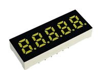
 数码管:基本概念、分类、技术发展及市场趋势

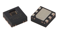
 湿度传感器:原理、选型、分类与特性

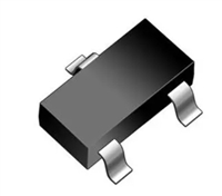
 解读SBAT54SLT1G手册:产品概述、参数分析

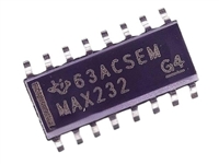
 MAX232DR资料:引脚说明、产品特性、电气参数
