Numonyx™ Embedded Flash Memory (J3 v. D)
Blocks are selectively and individually lockable in-system. Individual block locking uses
block lock-bits to lock and unlock blocks. Block lock-bits gate block erase and program
operations. Lock-bit configuration operations set and clear lock-bits (using the Set
Block Lock-Bit and Clear Block Lock-Bits commands).
The Status Register indicates when the WSM’s block erase, program, or lock-bit
configuration operation is finished.
The STS (STATUS) output gives an additional indicator of WSM activity by providing
both a hardware signal of status (versus software polling) and status masking
(interrupt masking for background block erase, for example). Status indication using
STS minimizes both CPU overhead and system power consumption. When configured in
level mode (default mode), it acts as a RY/BY# signal. When low, STS indicates that the
WSM is performing a block erase, program, or lock-bit configuration. STS-high indicates
that the WSM is ready for a new command, block erase is suspended (and
programming is inactive), program is suspended, or the device is in reset/power-down
mode. Additionally, the configuration command allows the STS signal to be configured
to pulse on completion of programming and/or block erases.
Three CE signals are used to enable and disable the device. A unique CE logic design
reduces decoder logic typically required for multi-chip designs. External logic is not
required when designing a single chip, a dual chip, or a 4-chip miniature card or SIMM
module.
The BYTE# signal allows either x8 or x16 read/writes to the device:
• BYTE#-low enables 8-bit mode; address A0 selects between the low byte and high
byte.
• BYTE#-high enables16-bit operation; address A1 becomes the lowest order
address and address A0 is not used (don’t care).
Figure 1, “Memory Block Diagram (32, 64 and 128 Mbit)” on page 10 shows a device
block diagram.
When the device is disabled, with CEx at VIH and RP# at VIH, the standby mode is
enabled. When RP# is at VIL, a further power-down mode is enabled which minimizes
power consumption and provides write protection during reset. A reset time (tPHQV) is
required from RP# going high until data outputs are valid. Likewise, the device has a
wake time (tPHWL) from RP#-high until writes to the CUI are recognized. With RP# at
VIL, the WSM is reset and the Status Register is cleared. (see Table 15, “Chip Enable
Truth Table” on page 31).
November 2007
308551-05
Datasheet
9


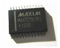
 MAX7219驱动8段数码管详解及数据手册关键信息

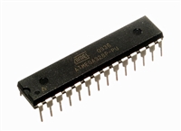
 ATMEGA328P技术资料深入分析

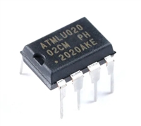
 AT24C02芯片手册管脚信息、参数分析、应用领域详解

 AT24C256芯片手册参数分析、引脚说明、读写程序示例
