
 5秒后页面跳转

| 是否Rohs认证: | 符合 | 生命周期: | Active |
| Reach Compliance Code: | unknown | 风险等级: | 5.62 |
| 老化: | 1 PPM/FIRST YEAR | 最大控制电压: | 2.5 V |
| 最小控制电压: | 0.5 V | 最长下降时间: | 8 ns |
| 频率调整-机械: | NO | 频率偏移/牵引率: | 10 ppm |
| 频率稳定性: | 0.1% | 安装特点: | SURFACE MOUNT |
| 端子数量: | 4 | 标称工作频率: | 20 MHz |
| 最高工作温度: | 70 °C | 最低工作温度: | |
| 振荡器类型: | CMOS | 输出负载: | 13.5 pF |
| 封装主体材料: | CERAMIC | 物理尺寸: | 5mmx3.2mmx1.45mm |
| 最长上升时间: | 8 ns | 最大压摆率: | 5 mA |
| 最大供电电压: | 3.465 V | 最小供电电压: | 3.135 V |
| 标称供电电压: | 3.3 V | 表面贴装: | YES |
| 最大对称度: | 55/45 % | 技术: | CMOS |
| Base Number Matches: | 1 |
| 型号 | 品牌 | 获取价格 | 描述 | 数据表 |
| X1G005061010100 | SEIKO |
获取价格 |
CMOS Output Clock Oscillator, |

|
| X1G005061010101 | SEIKO |
获取价格 |
CMOS Output Clock Oscillator, |
|
| X1G005061010300 | SEIKO |
获取价格 |
CMOS Output Clock Oscillator, |
|
| X1G005061010313 | SEIKO |
获取价格 |
CMOS Output Clock Oscillator, |
|
| X1G005071008601 | SEIKO |
获取价格 |
Clipped Sine Output Oscillator, |
|
| X1G005071008611 | SEIKO |
获取价格 |
Clipped Sine Output Oscillator, |
|
| X1G005071008612 | SEIKO |
获取价格 |
Clipped Sine Output Oscillator, |
|
| X1G005151012511 | SEIKO |
获取价格 |
Clipped Sine Output Oscillator, |
|
| X1G005151012512 | SEIKO |
获取价格 |
Clipped Sine Output Oscillator, |
|
| X1G005151015312 | SEIKO |
获取价格 |
Clipped Sine Output Oscillator, |
|
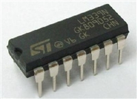 LM339N参数手册 :四路电压比较器的深度解读

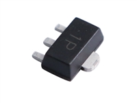 MMBT2222A资料手册:特性、应用、电气参数及替换型号推荐
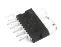 解读TDA7265手册资料:引脚说明 、电气参数及替换型号推荐
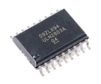 深入解读ULN2803A资料手册:引脚功能、电气参数、特性
工作时间:9:00-21:00
CEO邮箱:ceo@jiepei.com
投诉邮箱:tousu@jiepei.com


 浙公网安备 33010502006866号 浙ICP备10014259号-119
营业执照ICP证
浙公网安备 33010502006866号 浙ICP备10014259号-119
营业执照ICP证


