
 5秒后页面跳转

| 型号 | 品牌 | 描述 | 获取价格 | 数据表 |
| UT2309L-AE3-R | UTC | P-CHANNEL ENHANCEMENT MODE |
获取价格 |

|
| UT230GG-AE2-R | UTC | N-CHANNEL ENHANCEMENT MODE |
获取价格 |
|
| UT2311 | UTC | 20V P-CHANNEL ENHANCEMENT MODE MOSFET |
获取价格 |
|
| UT2311_15 | UTC | P-CHANNEL ENHANCEMENT MODE POWER MOSFET |
获取价格 |
|
| UT2311G-AE3-R | UTC | Power Field-Effect Transistor, 4A I(D), 20V, 0.055ohm, 1-Element, P-Channel, Silicon, Meta |
获取价格 |
|
| UT2311L-AE3-R | UTC | Power Field-Effect Transistor, 4A I(D), 20V, 0.055ohm, 1-Element, P-Channel, Silicon, Meta |
获取价格 |
|
 TJA1050资料数据分析、引脚说明、应用示例介绍

 DS3231时钟芯片:参数分析、引脚说明、应用示例介绍
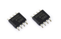 AD620资料手册解读:引脚说明及功能介绍、参数分析
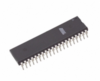 AT89C52资料手册:引脚说明、参数解读、LED流水灯控制程序示例
工作时间:9:00-21:00
CEO邮箱:ceo@jiepei.com
投诉邮箱:tousu@jiepei.com


 浙公网安备 33010502006866号 浙ICP备10014259号-119
营业执照ICP证
浙公网安备 33010502006866号 浙ICP备10014259号-119
营业执照ICP证


