
 5秒后页面跳转

| 型号 | 品牌 | 获取价格 | 描述 | 数据表 |
| TL494_05 | UTC |
获取价格 |
VOLTAGE MODE PWM CONTROL CIRCUIT |

|
| TL494_05 | ONSEMI |
获取价格 |
SWITCHMODE TM Pulse Width Modulation Control Circuit |
|
| TL494_07 | TI |
获取价格 |
PULSE-WIDTH-MODULATION CONTROL CIRCUITS |
|
| TL494_08 | HTC |
获取价格 |
Pulse-Width-Modulation Control Circuits |
|
| TL494_09 | UTC |
获取价格 |
VOLTAGE MODE PWM CONTROL CIRCUIT |
|
| TL494_10 | TI |
获取价格 |
PULSE-WIDTH-MODULATION CONTROL CIRCUITS |
|
| TL494_101 | TI |
获取价格 |
PULSE-WIDTH-MODULATION CONTROL CIRCUITS |
|
| TL494_12 | UTC |
获取价格 |
VOLTAGE MODE PWM CONTROL CIRCUIT |
|
| TL494_13 | UTC |
获取价格 |
VOLTAGE MODE PWM CONTROL CIRCUIT |
|
| TL494_15 | UTC |
获取价格 |
VOLTAGE MODE PWM CONTROL CIRCUIT |
|
 资料解读:TL494CN参数和引脚功能图说明

 什么是TL494芯片?TL494引脚图及功能、工作原理详解
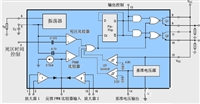
 解析光耦仿真器:升级光耦合器技术的必要性
 英伟达新一代Blackwell GPU过热问题致交付延迟
工作时间:9:00-21:00
CEO邮箱:ceo@jiepei.com
投诉邮箱:tousu@jiepei.com


 浙公网安备 33010502006866号 浙ICP备10014259号-119
营业执照ICP证
浙公网安备 33010502006866号 浙ICP备10014259号-119
营业执照ICP证


