
| 型号 | 品牌 | 获取价格 | 描述 | 数据表 |
| ST1500BAAJ-28.6363(T) | DIODES |
获取价格 |
VCXO, Clock, 1.5MHz Min, 100MHz Max, 28.6363MHz Nom, |

|
| ST1500BAAJ-FREQ1 | DIODES |
获取价格 |
HCMOS/TTL Output Clock Oscillator, 1.5MHz Min, 28.6363MHz Max, |
|
| ST1500BAAK-1.5000 | DIODES |
获取价格 |
VCXO, Clock, 1.5MHz Min, 100MHz Max, 1.5MHz Nom, |
|
| ST1500BAAK-1.5000(T) | DIODES |
获取价格 |
VCXO, Clock, 1.5MHz Min, 100MHz Max, 1.5MHz Nom, |
|
| ST1500BAAK-100.0000(T) | DIODES |
获取价格 |
VCXO, Clock, 1.5MHz Min, 100MHz Max, 100MHz Nom, |
|
| ST1500BAAK-28.6363(T) | DIODES |
获取价格 |
VCXO, Clock, 1.5MHz Min, 100MHz Max, 28.6363MHz Nom, |
|
| ST1500BAAK-FREQ2 | DIODES |
获取价格 |
HCMOS/TTL Output Clock Oscillator, 28.6363MHz Min, 70MHz Max, |
|
| ST1500BAAK-FREQ2(T) | DIODES |
获取价格 |
HCMOS/TTL Output Clock Oscillator, 28.6363MHz Min, 70MHz Max, |
|
| ST1500BAAK-FREQ2-OUT23 | DIODES |
获取价格 |
CMOS Output Clock Oscillator, 28.6363MHz Min, 70MHz Max, |
|
| ST1500BAAK-FREQ3(T) | DIODES |
获取价格 |
HCMOS/TTL Output Clock Oscillator, 70MHz Min, 100MHz Max, |
|
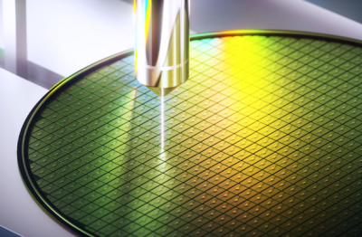 日本芯片代工厂JS Foundry濒临破产 激进扩张致负债161亿日元

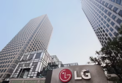 LG电子进军HBM制造关键领域 混合键合设备研发瞄准2028年量产
 博通10亿美元半导体工厂计划搁浅 西班牙谈判破裂背后暗藏政治变局
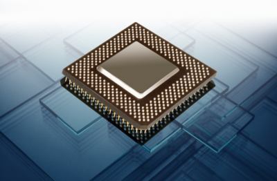 英特尔联手台积电2nm工艺 Nova Lake芯片流片完成引爆业界期待
工作时间:9:00-21:00
CEO邮箱:ceo@jiepei.com
投诉邮箱:tousu@jiepei.com


 浙公网安备 33010502006866号 浙ICP备10014259号-119
营业执照ICP证
浙公网安备 33010502006866号 浙ICP备10014259号-119
营业执照ICP证


