
| 型号 | 品牌 | 获取价格 | 描述 | 数据表 |
| SK320AQ-L | MCC |
获取价格 |
Tape: 5K/Reel, 80K/Ctn; |

|
| SK320B | TSC |
获取价格 |
3.0AMPS Surface Mount Schottky Barrier Rectifiers |
|
| SK320B | CZSTARSEA |
获取价格 |
SMBG |
|
| SK320BF | MDD |
获取价格 |
SURFACE MOUNT SCHOTTKY BARRIER RECTIFIER |
|
| SK320BFL | MCC |
获取价格 |
Tape&Reel: 5Kpcs/Reel; |
|
| SK320BG | CITC |
获取价格 |
Schottky Diodes |
|
| SK320BQ-L | MCC |
获取价格 |
Tape : 3K/Reel, 48K/Ctn; |
|
| SK320BTR | ETC |
获取价格 |
DIODE SCHOTTKY 200V 3A SMB |
|
| SK320C | CZSTARSEA |
获取价格 |
SMC |
|
| SK320C | WILLAS |
获取价格 |
3.0A SCHOTTKY BARRIER RECTIFIERS -20V- 200V SMC PACKAGE |
|
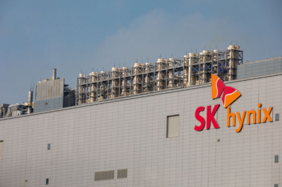 突破性进展!SK海力士全球首发量产型High NA EUV设备及高效散热DRAM

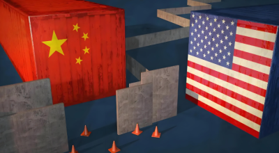 美国再次按下暂停键:GPU关税豁免3个月背后暗藏怎样的半导体
 宇树科技冲刺IPO,"杭州六小龙"即将登陆资本市场?
 台积电酝酿高端芯片涨价潮!苹果英伟达或面临成本压力
工作时间:9:00-21:00
CEO邮箱:ceo@jiepei.com
投诉邮箱:tousu@jiepei.com


 浙公网安备 33010502006866号 浙ICP备10014259号-119
营业执照ICP证
浙公网安备 33010502006866号 浙ICP备10014259号-119
营业执照ICP证


