
| 型号 | 品牌 | 获取价格 | 描述 | 数据表 |
| Q3614CE000097 | EPSON |
获取价格 |
Model : VG-4231CE; Frequency : 25.000000 MHz; LxWxH : 3.20 x 2.50 x 1.05 mm; |

|
| Q3614CE000098 | EPSON |
获取价格 |
Model : VG-4231CE; Frequency : 13.560000 MHz; LxWxH : 3.20 x 2.50 x 1.05 mm; |
|
| Q3614CE000099 | EPSON |
获取价格 |
Model : VG-4231CE; Frequency : 12.000000 MHz; LxWxH : 3.20 x 2.50 x 1.05 mm; |
|
| Q3620264 | PANDUIT |
获取价格 |
CRIMP SPLICER, STUB, NICKEL PLATED |
|
| Q36SR | DELTA |
获取价格 |
Industry standard footprint and pin out |
|
| Q36SR12017 | DELTA |
获取价格 |
Input Source Impedance |
|
| Q36SR12017NKFA | DELTA |
获取价格 |
Delphi Series Q36SR, Quarter Brick 204W DC/DC Power Modules: 18V~75Vin,12V, 17Aout |
|
| Q36SR12017NKFH | DELTA |
获取价格 |
Delphi Series Q36SR, Quarter Brick 204W DC/DC Power Modules: 18V~75Vin,12V, 17Aout |
|
| Q36SR12017NNFA | DELTA |
获取价格 |
Delphi Series Q36SR, Quarter Brick 204W DC/DC Power Modules: 18V~75Vin,12V, 17Aout |
|
| Q36SR12017NNFH | DELTA |
获取价格 |
Delphi Series Q36SR, Quarter Brick 204W DC/DC Power Modules: 18V~75Vin,12V, 17Aout |
|
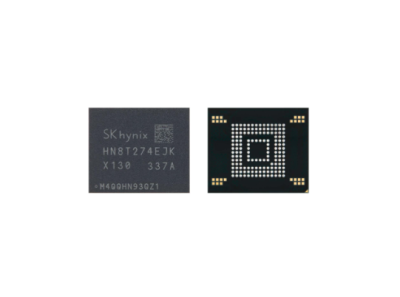 SK海力士再创纪录:全球首发高效散热移动DRAM技术揭秘

 欣旺达突破固态电池技术瓶颈:能量密度400Wh/kg方案验证完成
 英伟达财报净利润暴涨60%!H20芯片在中国市场零销售的背后
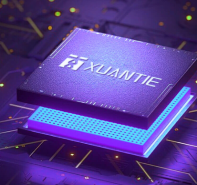 玄铁E901发布:全球最小RISC-V处理器如何颠覆嵌入式市
工作时间:9:00-21:00
CEO邮箱:ceo@jiepei.com
投诉邮箱:tousu@jiepei.com


 浙公网安备 33010502006866号 浙ICP备10014259号-119
营业执照ICP证
浙公网安备 33010502006866号 浙ICP备10014259号-119
营业执照ICP证


