
 5秒后页面跳转

| 型号 | 品牌 | 获取价格 | 描述 | 数据表 |
| P620-06QC | PLL |
获取价格 |
Low Phase Noise XO with multipliers (for 100-200MHz Fund or 3rdOT Xtal) |

|
| P620-06QCL | PLL |
获取价格 |
Low Phase Noise XO with multipliers (for 100-200MHz Fund or 3rdOT Xtal) |
|
| P620-07OC | PLL |
获取价格 |
Low Phase Noise XO with multipliers (for 100-200MHz Fund or 3rdOT Xtal) |
|
| P620-07OCL | PLL |
获取价格 |
Low Phase Noise XO with multipliers (for 100-200MHz Fund or 3rdOT Xtal) |
|
| P620-08OC | PLL |
获取价格 |
Low Phase Noise XO with multipliers (for 100-200MHz Fund or 3rdOT Xtal) |
|
| P620-08OCL | PLL |
获取价格 |
Low Phase Noise XO with multipliers (for 100-200MHz Fund or 3rdOT Xtal) |
|
| P620-08QC | PLL |
获取价格 |
Low Phase Noise XO with multipliers (for 100-200MHz Fund or 3rdOT Xtal) |
|
| P620-08QCL | PLL |
获取价格 |
Low Phase Noise XO with multipliers (for 100-200MHz Fund or 3rdOT Xtal) |
|
| P620-09OC | PLL |
获取价格 |
Low Phase Noise XO with multipliers (for 100-200MHz Fund or 3rdOT Xtal) |
|
| P620-09OCL | PLL |
获取价格 |
Low Phase Noise XO with multipliers (for 100-200MHz Fund or 3rdOT Xtal) |
|
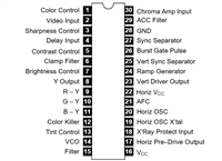 NTE1856手册解读:产品描、产品特性

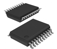 74HCT377资料手册解读:产品特性、引脚信息、参数分析
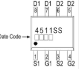 GSS4511手册快速解读:产品特性、参数分析
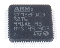 STM32F1038资料手册解读:产品特性、引脚信息、数据参数
工作时间:9:00-21:00
CEO邮箱:ceo@jiepei.com
投诉邮箱:tousu@jiepei.com


 浙公网安备 33010502006866号 浙ICP备10014259号-119
营业执照ICP证
浙公网安备 33010502006866号 浙ICP备10014259号-119
营业执照ICP证


