Data Sheet
November 2006
ORCA Series 3C and 3T FPGAs
Table of Contents
Contents
Page
Contents
Page
Features ......................................................................1
System-Level Features................................................4
Description...................................................................5
FPGA Overview ..........................................................5
PLC Logic ...................................................................5
Description (continued)................................................6
PIC Logic ....................................................................6
System Features ........................................................6
Routing .......................................................................6
Configuration ..............................................................6
Description (continued)................................................7
ispLEVER Development System ................................7
Architecture .................................................................7
Programmable Logic Cells ..........................................9
Programmable Function Unit ......................................9
Look-Up Table Operating Modes .............................11
Supplemental Logic and Interconnect Cell (SLIC).....19
PLC Latches/Flip-Flops ............................................23
PLC Routing Resources ...........................................25
PLC Architectural Description ...................................32
rogrammable Input/Output Cells................................34
5 V Tolerant I/O ........................................................35
PCI Compliant I/O .....................................................35
Inputs ........................................................................36
Outputs .....................................................................39
PIC Routing Resources ............................................42
PIC Architectural Description ....................................43
High-Level Routing Resources..................................45
Interquad Routing .....................................................45
Programmable Corner Cell Routing .........................46
PIC Interquad (MID) Routing ....................................47
Clock Distribution Network ........................................48
PFU Clock Sources ..................................................48
Clock Distribution in the PLC Array ..........................49
Clock Sources to the PLC Array ...............................50
Clocks in the PICs ....................................................50
ExpressCLK Inputs ...................................................51
Selecting Clock Input Pins ........................................51
Special Function Blocks ............................................52
Single Function Blocks .............................................52
Boundary Scan .........................................................55
Microprocessor Interface (MPI) .................................62
PowerPC System .....................................................63
i960 System ..............................................................64
MPI Interface to FPGA .............................................65
MPI Setup and Control .............................................66
Programmable Clock Manager (PCM) ......................70
PCM Registers .........................................................71
Delay-Locked Loop (DLL) Mode ...............................73
Phase-Locked Loop (PLL) Mode ..............................74
PCM/FPGA Internal Interface ...................................77
PCM Operation .........................................................77
2
PCM Detailed Programming .................................... 78
PCM Applications .................................................... 81
PCM Cautions ......................................................... 82
FPGA States of Operation........................................ 83
Initialization .............................................................. 83
Configuration ........................................................... 84
Start-Up ................................................................... 85
Reconfiguration ....................................................... 86
Partial Reconfiguration ............................................ 86
Other Configuration Options .................................... 86
Using ispLEVER to Generate
Configuration RAM Data ....................................... 87
Configuration Data Frame ....................................... 87
Bit Stream Error Checking ....................................... 89
FPGA Configuration Modes...................................... 90
Master Parallel Mode ............................................... 90
Master Serial Mode ................................................. 91
Asynchronous Peripheral Mode .............................. 92
Microprocessor Interface (MPI) Mode ..................... 92
Slave Serial Mode ................................................... 95
Slave Parallel Mode ................................................. 95
Daisy-Chaining ........................................................ 96
Daisy-Chaining with Boundary Scan ....................... 97
Absolute Maximum Ratings...................................... 98
Recommended Operating Conditions ..................... 98
Electrical Characteristics .......................................... 99
Timing Characteristic Description .......................... 101
Description ............................................................. 101
PFU Timing ........................................................... 102
PLC Timing ............................................................ 109
SLIC Timing ........................................................... 109
PIO Timing ............................................................. 110
Special Function Blocks Timing ............................. 113
Clock Timing .......................................................... 121
Configuration Timing ............................................. 131
Readback Timing ................................................... 140
Input/Output Buffer Measurement Conditions ........ 141
Output Buffer Characteristics ................................. 142
OR3Cxx ................................................................. 142
OR3Txxx ................................................................ 143
Estimating Power Dissipation................................. 144
OR3Cxx ................................................................. 144
OR3Txxx................................................................. 145
Pin Information ....................................................... 147
Pin Descriptions...................................................... 147
Package Compatibility ........................................... 151
Compatibility with OR2C/TxxA Series .................... 152
Package Thermal Characteristics........................... 188
FPGA Maximum Junction Temperature ................ 190
Package Coplanarity .............................................. 191
Package Parasitics................................................. 191
Package Outline Diagrams..................................... 192
Lattice Semiconductor

 5秒后页面跳转


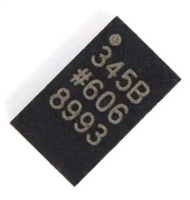 ADXL345传感器工作原理、参数分析、引脚说明

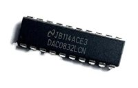 一文带你了解,DAC0832工作原理、输出电压范围、分辨率等参数
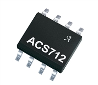 ACS712电流检测使用指南及资料手册参数分析
 TLP521资料手册解读:参数分析、引脚说明、典型电路


 浙公网安备 33010502006866号 浙ICP备10014259号-119
营业执照ICP证
浙公网安备 33010502006866号 浙ICP备10014259号-119
营业执照ICP证


