
 5秒后页面跳转

| 型号 | 品牌 | 获取价格 | 描述 | 数据表 |
| NL17SV16XV5T2 | ONSEMI |
获取价格 |
Ultra-Low Voltage Buffer |

|
| NL17SV16XV5T2_05 | ONSEMI |
获取价格 |
Ultra−Low Voltage Buffer |
|
| NL17SV16XV5T2G | ONSEMI |
获取价格 |
Ultra−Low Voltage Buffer |
|
| NL17SV32-D | ONSEMI |
获取价格 |
Single Gate 2-Input OR Gate |
|
| NL17SV32XV5T2 | ONSEMI |
获取价格 |
Single Gate 2−Input OR Gate |
|
| NL17SV32XV5T2_05 | ONSEMI |
获取价格 |
Single Gate 2−Input OR Gate |
|
| NL17SV32XV5T2G | ONSEMI |
获取价格 |
Single Gate 2−Input OR Gate |
|
| NL17SZ00 | ONSEMI |
获取价格 |
Single 2-Input NAND Gate |
|
| NL17SZ00/D | ETC |
获取价格 |
Single 2-Input NAND Gate |
|
| NL17SZ00_06 | ONSEMI |
获取价格 |
Single 2−Input NAND Gate |
|
 STS5DNE30L资料手册解读:参数分析、特性与应用

 MDU1511资料手册解读:探索这款MOSFET的全面特性
 2SB1260资料手册解读:电气参数、产品特性
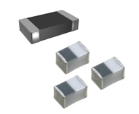 掌握电感选型:关键参数Q值全解析
工作时间:9:00-21:00
CEO邮箱:ceo@jiepei.com
投诉邮箱:tousu@jiepei.com


 浙公网安备 33010502006866号 浙ICP备10014259号-119
营业执照ICP证
浙公网安备 33010502006866号 浙ICP备10014259号-119
营业执照ICP证


