19-2220; Rev 1; 11/04
1 :5 Diffe re n t ia l LVP ECL/LVECL/HS TL
Clo c k a n d Da t a Drive r
Ge n e ra l De s c rip t io n
Fe a t u re s
The MAX9315 low-skew, 1-to-5 differential driver is
designed for clock and data distribution. This device
allows selection between two inputs. The selected input
is reproduced at five differential outputs. The differential
inputs can be adapted to accept a single-ended input
♦ +2.375V to +3.8V Supply for Differential
HSTL/LVPECL Operation
♦ -2.375V to -3.8V Supply for Differential LVECL
Operation
by connecting the on-chip V supply to one input as a
reference voltage.
BB
♦ Two Selectable Differential Inputs
♦ Synchronous Output Enable/Disable
♦ 20ps Output-to-Output Skew
The MAX9315 fe a ture s low outp ut-to-outp ut s ke w
(20ps), making it ideal for clock and data distribution
across a backplane or a board. For interfacing to differ-
ential HSTL and LVPECL signals, this device operates
over a +2.375V to +3.8V supply range, allowing high-
performance clock or data distribution in systems with a
nominal +2.5V or +3.3V supply. For differential LVECL
operation, this device operates with a -2.375V to -3.8V
supply.
♦ 360ps Propagation Delay
♦ Guaranteed 400mV Differential Output at 1.5GHz
♦ On-Chip Reference for Single-Ended Inputs
♦ Input Biased Low when Left Open
♦ Pin Compatible with MC100LVEP14
The MAX9315 is offe re d in a s p a c e -s a ving 20-p in
TSSOP package.
Ap p lic a t io n s
Ord e rin g In fo rm a t io n
Precision Clock Distribution
Low-Jitter Data Repeater
Data and Clock Driver and Buffer
Central Office Backplane Clock Distribution
DSLAM Backplane
PART
TEMP RANGE
PIN-PACKAGE
MAX9315EUP
-40°C to +85°C
20 TSSOP
P in Co n fig u ra t io n
Base Station
ATE
MAX9315
Typ ic a l Ap p lic a t io n Circ u it
TOP VIEW
QO
Q0
Q1
Q1
Q2
Q2
Q3
Q3
Q4
1
2
3
4
5
6
7
8
9
20
19 EN
18
V
CC
D
Q
V
CC
RECEIVER
MAX9315
17 CLK1
16 CLK1
Z
Z
= 50Ω
= 50Ω
O
O
Q_
Q_
15
14
V
BB
CLK0
13 CLK0
12 SEL
50Ω
50Ω
Q4 10
11 V
EE
V
= V - 2.0V
CC
TT
TSSOP
Functional Diagram appears at end of data sheet.
________________________________________________________________ Maxim Integrated Products
1
For pricing, delivery, and ordering information, please contact Maxim/Dallas Direct! at
1-888-629-4642, or visit Maxim’s website at www.maxim-ic.com.


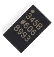
 ADXL345传感器工作原理、参数分析、引脚说明

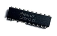
 一文带你了解,DAC0832工作原理、输出电压范围、分辨率等参数

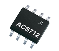
 ACS712电流检测使用指南及资料手册参数分析

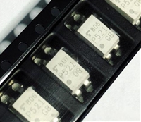
 TLP521资料手册解读:参数分析、引脚说明、典型电路
