
 5秒后页面跳转

| 是否无铅: | 含铅 | 是否Rohs认证: | 不符合 |
| 生命周期: | Obsolete | 零件包装代码: | QFN |
| 包装说明: | HVQCCN, | 针数: | 24 |
| Reach Compliance Code: | not_compliant | HTS代码: | 8542.39.00.01 |
| 风险等级: | 5.42 | 应用程序: | SONET;SDH |
| JESD-30 代码: | S-XQCC-N24 | JESD-609代码: | e0 |
| 长度: | 4 mm | 湿度敏感等级: | 1 |
| 负电源额定电压: | -5.2 V | 功能数量: | 1 |
| 端子数量: | 24 | 最高工作温度: | 85 °C |
| 最低工作温度: | -40 °C | 封装主体材料: | UNSPECIFIED |
| 封装代码: | HVQCCN | 封装形状: | SQUARE |
| 封装形式: | CHIP CARRIER, HEAT SINK/SLUG, VERY THIN PROFILE | 峰值回流温度(摄氏度): | 245 |
| 认证状态: | Not Qualified | 座面最大高度: | 0.8 mm |
| 表面贴装: | YES | 技术: | BIPOLAR |
| 电信集成电路类型: | ATM/SONET/SDH SUPPORT CIRCUIT | 温度等级: | INDUSTRIAL |
| 端子面层: | Tin/Lead (Sn/Pb) | 端子形式: | NO LEAD |
| 端子节距: | 0.5 mm | 端子位置: | QUAD |
| 处于峰值回流温度下的最长时间: | NOT SPECIFIED | 宽度: | 4 mm |
| 型号 | 品牌 | 描述 | 获取价格 | 数据表 |
| MAX3945 | ADI | 1.0625Gbps至11.3Gbps、SFP+双通道限幅放大器 |
获取价格 |

|
| MAX3945ETE | MAXIM | 1.0625Gbps to 11.3Gbps, SFP Dual-Path Limiting Amplifier |
获取价格 |
|
| MAX3945ETE+ | MAXIM | Clock Recovery Circuit, 1-Func, CMOS, 3 X 3 MM, 0.80 MM HEIGHT, ROHS COMPLIANT, TQFN-16 |
获取价格 |
|
| MAX3945ETE+T | MAXIM | ATM/SONET/SDH IC, 1-Func, PQCC16, |
获取价格 |
|
| MAX3946 | MAXIM | 1.0625Gbps to 11.3Gbps, SFP+ Laser Driver with Laser Impedance Mismatch Tolerance |
获取价格 |
|
| MAX3946_11 | MAXIM | 1Gbps to 11.3Gbps, SFP+ Laser Driver with Laser Impedance Mismatch Tolerance |
获取价格 |
|
| MAX3946ETG | MAXIM | 1Gbps to 11.3Gbps, SFP+ Laser Driver with Laser Impedance Mismatch Tolerance |
获取价格 |
|
| MAX3946ETG+ | MAXIM | 1.0625Gbps to 11.3Gbps, SFP+ Laser Driver with Laser Impedance Mismatch Tolerance |
获取价格 |
|
| MAX3946ETG+T | MAXIM | Telecom Circuit, 1-Func, Bipolar, ROHS COMPLIANT, TQFN-24 |
获取价格 |
|
| MAX3948 | MAXIM | 11.3Gbps, Low-Power, DC-Coupled Laser Driver |
获取价格 |
|
| MAX3948 | ADI | 11.3Gbps低功耗直流耦合激光驱动器 |
获取价格 |
|
| MAX3948ETE+ | MAXIM | 11.3Gbps, Low-Power, DC-Coupled Laser Driver |
获取价格 |
|
| MAX3949 | ADI | 11.3Gbps、低功耗、交流耦合激光驱动器 |
获取价格 |
|
| MAX3949ETE+ | MAXIM | 1GBPS TO 11.3GBPS, SFP+ LASER DRIVER |
获取价格 |
|
| MAX394C/D | MAXIM | Low-Voltage, Quad, SPDT, CMOS Analog Switch |
获取价格 |
|
| MAX394CAP+ | MAXIM | 暂无描述 |
获取价格 |
|
| MAX394CPP | MAXIM | Low-Voltage, Quad, SPDT, CMOS Analog Switch |
获取价格 |
|
| MAX394CPP+ | MAXIM | SPDT, 4 Func, 1 Channel, CMOS, PDIP20, 0.300 INCH, ROHS COMPLIANT, PLASTIC, DIP-20 |
获取价格 |
|
| MAX394CWP | MAXIM | Low-Voltage, Quad, SPDT, CMOS Analog Switch |
获取价格 |
|
| MAX394EAP | MAXIM | SPDT, 4 Func, 1 Channel, CMOS, PDSO20, 0.209 INCH, SSOP-20 |
获取价格 |
|
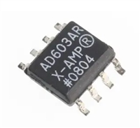 AD603资料手册解读:封装、引脚功能及电气参数全面分析

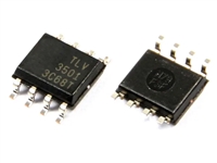 TLV3501高性能比较器详解:封装、引脚说明及替代型号推荐
 热敏电阻型号命名规则的深度解析
 晶闸管控制角与电压关系专业性解答
工作时间:9:00-21:00
CEO邮箱:ceo@jiepei.com
投诉邮箱:tousu@jiepei.com


 浙公网安备 33010502006866号 浙ICP备10014259号-119
营业执照ICP证
浙公网安备 33010502006866号 浙ICP备10014259号-119
营业执照ICP证


