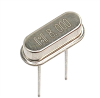
J-Type Voltage Controlled Crystal Oscillator
Table 7. Standard Frequencies, in MHz, for CMOS output option
1.024
3.686
1.544
4.000
2.000
4.032
2.048
4.096
3.088
4.434
3.580
5.000
6.144
6.176
6.312
6.400
8.000
8.192
8.448
10.000
15.360
20.000
30.000
40.000
62.208
12.000
15.440
20.480
32.000
40.960
65.536
12.288
16.000
24.000
32.768
44.736
77.760
12.352
16.384
24.576
34.368
50.000
155.5201
13.000
18.432
24.704
35.328
51.840
14.318
19.440
27.000
38.880
52.000
1. Uses a PLL multiplier, jitter is 25ps rms typical vs 3ps typical for a HFF design
Other frequencies available upon request.
Table 8. Pin Out Information for the PECL output option
6
5
4
Pin
Symbol
Function
1
2
3
4
5
6
VC
VCXO Control Voltage
N/C or E/D2
GND
No Connect or Output Disable
Case and Electrical Ground
VCXO Output
TOP VIEW
Output
COutput
VCC
1
2
3
VCXO Complementary Output
Power Supply Voltage (5.0 V or 3.3 V ±10%)
. By setting OD high, the outputs are disabled and OUT is held low while Complementary OUT is held high. Output is enabled if E/D
< VCC-1.6V,
2. See ordering information for enable/disable option.
Table 9. Electrical Performance @ 25°C for the PECL output option
Parameter
Supply Voltage 1, +5 volt option
+3.3 volt option
Symbol
Minimum
4.5
Typical
5.0
Maximum
5.5
Units
V
V
3.0
3.3
3.6
Supply Current
frequency dependent
Center Frequency, see ordering information
Operating Temperature, see ordering info
Absolute Pull Range over the operating
temperature range, aging and power supply.
Vc= 0.5 to 4.5 or 0.3 to 3.0
see ordering information for options
Gain Transfer
FN
TOP
APR
15
170
MHz
°C
ppm
0/70, -40/85
±32, ±50
KV
Positive
(Frequency vs. Control Voltage)
Output Level High2
VOH
VOL
Vcc-1.025
Vcc-1.810
-
-
Vcc-0.880
Vcc-1.620
V
V
Output Level Low2
Output Logic Levels for -40 to 85°C Operation
Output Level High2
VOH
VOL
tR/tf
SYM
IL
Vcc-1.085
Vcc-1.830
Vcc-0.880
Vcc-1.555
1
V
V
ns
Output Level Low2
Output Rise and Fall Time2
Duty Cycle3, see ordering info
Input Leakage
45/55
0.1
%
mA
pS
kHz
<1
RMS Jitter, 12kHz to 20 MHz, P option (HFF)
Control Voltage Modulation Bandwidth
Maximum Control Voltage
Maximum Supply Voltage
Storage Temperature
BW
10
0
VDD
7
125
V
°C
°C/s
TS
TLS
-55
-
-
-
Soldering Temp./Time
240/10
1. Power supply bypass is required and a 0.1uF in parallel with a 0.01uF high frequency capacitor is recommended.
2. Transition times are measured from 20% to 80% of a full 10K ECL level swing.
Vectron International 267 Lowell Rd. Hudson, NH 03051 Tel:1-88-VECTRON-1
e-mail vectron@vectron.com
6


 资料手册解读:UC3842参数和管脚说明

 一文带你了解无源晶振的负载电容为何要加两颗谐振电容CL1和CL2

 玻璃管保险丝与陶瓷管保险丝:区别与替代性探讨

 PCF8574资料解读:主要参数分析、引脚说明
