
| 型号 | 品牌 | 获取价格 | 描述 | 数据表 |
| FMV30N60S1FD | FUJI |
获取价格 |
TO-220F(SLS) |

|
| FMV32 | 3M |
获取价格 |
3M⢠Void Polyester Label Products |
|
| FMV35N60S1 | FUJI |
获取价格 |
TO-220F(SLS) |
|
| FMV35N60S1FD | FUJI |
获取价格 |
TO-220F(SLS) |
|
| FMV40N60S1 | FUJI |
获取价格 |
TO-220F(SLS) |
|
| FMV60N070S2HF | FUJI |
获取价格 |
TO-220F(SLS) |
|
| FMV60N075S2FDHF | FUJI |
获取价格 |
TO-220F(SLS) |
|
| FMV60N079S2HF | FUJI |
获取价格 |
TO-220F(SLS) |
|
| FMV60N084S2FDHF | FUJI |
获取价格 |
TO-220F(SLS) |
|
| FMV60N088S2HF | FUJI |
获取价格 |
TO-220F(SLS) |
|
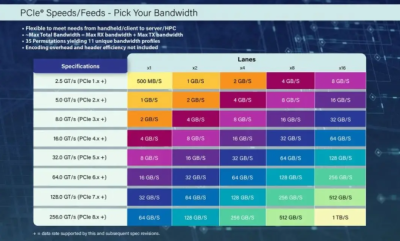 PCIe 8.0规范草案获里程碑进展:256GT/s速率开启1TB/s带宽时代

 寒武纪紧急辟谣背后:AI芯片龙头的真实现状与投资陷阱
 英伟达50亿入股英特尔:芯片巨头联手剑指AMD,行业格局生变
 闪迪预警:NAND闪存供应短缺将持续至2026年
工作时间:9:00-21:00
CEO邮箱:ceo@jiepei.com
投诉邮箱:tousu@jiepei.com


 浙公网安备 33010502006866号 浙ICP备10014259号-119
营业执照ICP证
浙公网安备 33010502006866号 浙ICP备10014259号-119
营业执照ICP证


