
 5秒后页面跳转

| 型号 | 品牌 | 获取价格 | 描述 | 数据表 |
| FM25W04 | FM |
获取价格 |
SPI NOR Flash |

|
| FM25W16 | FM |
获取价格 |
SPI NOR Flash |
|
| FM25W256 | RAMTRON |
获取价格 |
256Kb Wide Voltage SPI F-RAM |
|
| FM25W256_13 | CYPRESS |
获取价格 |
256Kb Wide Voltage SPI F-RAM |
|
| FM25W256-G | CYPRESS |
获取价格 |
256Kb Wide Voltage SPI F-RAM |
|
| FM25W256-G | RAMTRON |
获取价格 |
256Kb Wide Voltage SPI F-RAM |
|
| FM25W256-G | INFINEON |
获取价格 |
铁电存储器 (F-RAM) |
|
| FM25W256-GTR | RAMTRON |
获取价格 |
256Kb Wide Voltage SPI F-RAM |
|
| FM25W256-GTR | CYPRESS |
获取价格 |
256Kb Wide Voltage SPI F-RAM |
|
| FM25W256-GTR | INFINEON |
获取价格 |
铁电存储器 (F-RAM) |
|
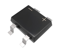 数据手册解读:MB10S引脚说明、电气参数

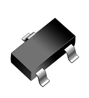 2N7002K资料解读:产品特性和型号推荐
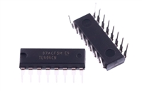 资料解读:TL494CN参数和引脚功能图说明
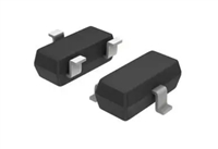 解读BAT54A数据手册:全面解析产品特性与应用
工作时间:9:00-21:00
CEO邮箱:ceo@jiepei.com
投诉邮箱:tousu@jiepei.com


 浙公网安备 33010502006866号 浙ICP备10014259号-119
营业执照ICP证
浙公网安备 33010502006866号 浙ICP备10014259号-119
营业执照ICP证


