CYWT1543AV18
CYWT1545AV18
72-Mbit QDR® II+ SRAM Four-Word Burst
Architecture (2.0 Cycle Read Latency)
Features
Configurations
■ Separate independent read and write data ports
❐ Supports concurrent transactions
With Read Cycle Latency of 2.0 cycles:
CYWT1543AV18 – 4M x 18
■ 250-MHz clock for high bandwidth
CYWT1545AV18 – 2M x 36
■ Four-word burst for reducing address bus frequency
Functional Description
■ DoubleDataRate(DDR)interfacesonbothreadandwriteports
(data transferred at 500 MHz) at 250 MHz
The CYWT1543AV18 and CYWT1545AV18 are 1.8 V
synchronous pipelined SRAMs, equipped with QDR II+ archi-
tecture. Similar to QDR II architecture, QDR II+ SRAMs consists
of two separate ports: the read port and the write port to access
the memory array. The read port has dedicated data outputs to
support read operations and the write port has dedicated data
inputs to support write operations. QDR II+ architecture has
separate data inputs and data outputs to completely eliminate
the need to “turn around” the data bus that exists with common
I/O devices. Each port is accessed through a common address
bus. Addresses for read and write addresses are latched on
alternate rising edges of the input (K) clock. Accesses to the
QDR II+ read and write ports are completely independent of one
another. To maximize data throughput, both read and write ports
are equipped with DDR interfaces. Each address location is
associated with four 18-bit words (CYWT1543AV18) or 36-bit
words (CYWT1545AV18) that burst sequentially into or out of the
device. Because data is transferred into and out of the device on
every rising edge of both input clocks (K and K), memory
bandwidth is maximized while simplifying system design by
eliminating bus “turn-arounds”.
■ Available in 2.0 clock cycle latency
■ Two input clocks (K and K) for precise DDR timing
❐ SRAM uses rising edges only
■ Echo clocks (CQ and CQ) simplify data capture in high-speed
systems
■ Data valid pin (QVLD) to indicate valid data on the output
■ Single multiplexed address input bus latches address inputs
for both read and write ports
■ Separate port selects for depth expansion
■ Synchronous internally self-timed writes
■ Available in x18 and x36 configurations
■ Full data coherency, providing most current data
[1]
■ Core VDD = 1.8 V ± 0.1 V; I/O VDDQ = 1.4 V to VDD
■ HSTL inputs and variable drive HSTL output buffers
■ Available in 165-pin CCGA package (21 x 25 x 2.89 mm)
■ Offered with 0.51 mm Sn/Pb solder columns
Depth expansion is accomplished with port selects, which
enables each port to operate independently.
All synchronous inputs pass through input registers controlled by
the K or K input clocks. All data outputs pass through output
registers controlled by the K or K input clocks. Writes are
conducted with on-chip synchronous self-timed write circuitry.
■ JTAG 1149.1 compatible test access port
■ Delay Lock Loop (DLL) for accurate data placement
Selection Guide
Description
250 MHz
250
Unit
Maximum Operating Frequency
MHz
x18
x36
1100
Maximum Operating Current
mA
1140
Note
1. The QDR consortium specification for V
is 1.5 V + 0.1 V. The Cypress QDR devices exceed the QDR consortium specification and are capable of supporting
DDQ
V
= 1.4 V to V
.
DDQ
DD
Cypress Semiconductor Corporation
Document Number: 002-18432 Rev. **
•
198 Champion Court
•
San Jose, CA 95134-1709
•
408-943-2600
Revised February 23, 2017


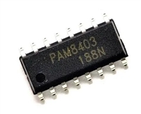
 PAM8403音频功率放大器:资料手册参数分析

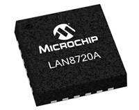
 LAN8720以太网收发器:资料手册参数分析

 SI2301 N沟道MOSFET:资料手册参数分析

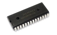
 ADC0809逐次逼近寄存器型模数转换器:资料手册参数分析
