CYWT1543AV18
CYWT1545AV18
Pin Definitions
Pin Name
I/O
Pin Description
D[x:0]
Input-
Data Input Signals. Sampled on the rising edge of K and K clocks
.
when valid write operations are active
Synchronous CYWT1543AV18 D[17:0]
CYWT1545AV18 D[35:0]
WPS
Input-
Write Port Select Active LOW. Sampled on the rising edge of the K clock. When asserted active, a
Synchronous write operation is initiated. Deasserting deselects the write port. Deselecting the write port ignores D[x:0]
.
BWS0,
BWS1,
BWS2,
BWS3
Input-
Synchronous
Byte Write Select 0, 1, 2, and 3 Active LOW.
Sampled on the rising edge of the K and K clocks when
write operations are active. Used to select which byte is written into the device during the current portion
of the write operations. Bytes not written remain unaltered.
CYWT1543AV18 BWS0 controls D[8:0] and BWS1 controls D[17:9].
CYWT1545AV18 BWS0 controls D[8:0], BWS1 controls D[17:9]
,
BWS2 controls D[26:18] and BWS3 controls D[35:27].
All the Byte Write Selects are sampled on the same edge as the data. Deselecting a Byte Write Select
ignores the corresponding byte of data and it is not written into the device
.
A
Input-
Address Inputs. Sampled on the rising edge of the K clock during active read and write operations. These
Synchronous address inputs are multiplexed for both read and write operations. Internally, the device is organized as
4M x 18 (four arrays each of 1M x 18) for CYWT1543AV18 and 2M x 36 (four arrays each of 512K x 36)
for CYWT1545AV18. Therefore, only 20 address inputs are needed to access the entire memory array
of CYWT1543AV18 and 19 address inputs for CYWT1545AV18. These inputs are ignored when the
appropriate port is deselected.
Q[x:0]
Outputs-
Data Output Signals. These pins drive out the requested data when the read operation is active. Valid
Synchronous data is driven out on the rising edge of the K and K clocks during read operations. On deselecting the
read port, Q[x:0] are automatically tristated.
CYWT1543AV18 Q[17:0]
CYWT1545AV18 Q[35:0]
RPS
Input-
Read Port Select Active LOW. Sampled on the rising edge of positive input clock (K). When active, a
Synchronous read operation is initiated. Deasserting deselects the read port. When deselected, the pending access is
allowed to complete and the output drivers are automatically tristated following the next rising edge of the
K clock. Each read access consists of a burst of four sequential transfers.
QVLD
K
Valid output Valid Output Indicator. The Q Valid indicates valid output data. QVLD is edge-aligned with CQ and CQ.
indicator
Input-
Clock
Positive Input Clock Input. The rising edge of K is used to capture synchronous inputs to the device
and to drive out data through Q[x:0]. All accesses are initiated on the rising edge of K.
K
Input-
Clock
Negative Input Clock Input. K is used to capture synchronous inputs being presented to the device and
to drive out data through Q[x:0]
.
CQ
CQ
ZQ
Echo Clock Synchronous Echo Clock Outputs. This is a free-running clock and is synchronized to the input clock
(K) of the QDR II+. The timings for the echo clocks are shown in the Switching Characteristics on page 22.
Echo Clock Synchronous Echo Clock Outputs. This is a free-running clock and is synchronized to the input clock
(K) of the QDR II+. The timings for the echo clocks are shown in the Switching Characteristics on page 22.
Input
Output Impedance Matching Input. This input is used to tune the device outputs to the system data bus
impedance. CQ, CQ, and Q[x:0] output impedance are set to 0.2 x RQ, where RQ is a resistor connected
between ZQ and ground. Alternatively, this pin can be connected directly to VDDQ, which enables the
minimum impedance mode. This pin cannot be connected directly to GND or left unconnected.
DOFF
Input
DLL Turn Off Active LOW. Connecting this pin to ground turns off the DLL inside the device. The
timings in the DLL turned off operation are different from those listed in this data sheet. For normal
operation, this pin can be connected to a pull-up through a 10-k or less pull-up resistor. The device
behaves in QDR I mode when the DLL is turned off. In this mode, the device can be operated at a
frequency of up to 167 MHz with QDR I timing.
TDO
TCK
TDI
Output
Input
TDO for JTAG.
TCK Pin for JTAG.
TDI Pin for JTAG.
Input
Document Number: 002-18432 Rev. **
Page 5 of 26


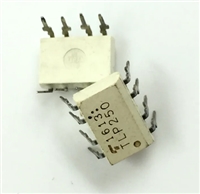
 TLP250光耦合器:资料手册参数分析

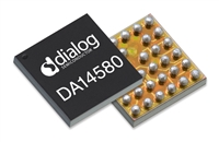
 DA14580 低功耗蓝牙系统级芯片(SoC):资料手册参数分析

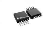
 INA226 高精度电流和功率监控器:资料手册参数分析

 SI2302 N沟道MOSFET:资料手册参数分析
