PRELIMINARY
CY7C955
Receive Clock Recovery (continued)
Name
Pin
I/O
Description
RXDO±
22−23
Differential Out Receive Output Data: These differential outputs represent the retimed version of the
input data stream (RXD±) in normal mode and the buffered version of the input datas-
tream (RXD±) in bypass mode. This output pair can be used as inputs to decision
feedback equalizers to correct for baseline wander. RXDO can be turned off to save
power by setting RXDOD (Reg−04H, bit 7) to 1.
RRCLK±
33−34
Differential In
Receive Clock: These inputs are used to clock in the differential data (RXD±) when the
Receive clock recovery block is bypassed (RBYP=HIGH). If RBYP is LOW, RRCLK is
multiplied by 8, 24, or 8/3 depending on the setting of RREFSEL (Reg−07H, bit 0) and
use as a reference for the Receiver PLL. Refer to the section on “Interface Termination
and Bias of Schemes” for connection examples to these pins.
RBYP
41
Input
Receive Clock Bypass: When this input is HIGH the Receiver clock recovery block is
bypassed. In this mode the device does not recover clock and data from the Receive
input data stream (RXD±) but instead uses the RRCLK± inputs to clock the differential
data into the device. When this input is LOW the Receiver clock recovery block recovers
the clock and data from the input data stream. In this mode a byte-rate clock is expected
on the RRCLK± inputs.
RCLK
RFP
57
58
Output
Output
Receive Byte Reference: Provides a byte-rate reference derived from the recovered
bit- rate Receive clock. RALM, RCP, and RGFC are aligned with this clock.
Receive Frame Reference: This output provides a frame-rate reference clock aligned
to the SONET/SDH frame alignment bytes. RFP will pulse HIGH for one RCLK cycle
every 125 seconds even at OOF and LOF situations.
LF+
42
Input
Input
NC. This pin is for factory testing only.
LF–, LFO
43, 44
These are the PLL filter pins. Connect a 0.47-µF capacitor across LF– and LFO.
Receive ATM Interface
Name
Pin
I/O
Description
RGFC
59
Output
Receive Generic Flow Control: This output provides the four bits of the current ATM
cell header GFC locations at each successive RCLK pulse. The RCP output indicates
the first GFC bit location. This output is forced LOW if the ATM Cell Processor has lost
cell delineation.
RALM
RCP
63
60
Output
Output
Receive Interrupt: This active HIGH signal is aligned with the RCLK byte-rate clock and
signals the presence of LAIS, PAIS, LOS, LOF, LOP, or LCD.
Receive Start Of GFC: This output indicates the first bit of the GFC presented on the
RGFC output. This output goes HIGH for 1 RCLK cycle 6 byte times after the corre-
sponding cell is written into the Receive FIFO.
Receive Utopia Interface
Name
Pin No I/O
Description
RDAT[7:0] 70−71
74−79
Output
Output
Output
Input
Receive Utopia Data: Byte-wide data driven from the PHY to ATM layer. RDAT[7] is the
MSB
RPRTY
RSOC
RFCLK
82
83
67
Receive Utopia Data Parity: Data parity calculated over RDAT[7:0]. Odd parity is as-
sumed unless the TXPRTY bit is set to even parity by Reg−50H, bit 6.
Receive Utopia Start of Cell: Asserted HIGH when RDAT[7:0] contains the first byte of
an ATM cell.
Receive Utopia Clock: Data transfer clock. Data is transferred from the AX on the rising
edge of RFCLK when RRDENB is asserted (LOW).
RRDENB
RCA
68
69
Input
Receive Utopia Enable: Enables the RFCLK input for data transfers from the AX.
Output
Receive Utopia Cell Available: An active signal indicates that the Receive FIFO con-
tains at least 1 or 4 more bytes of data. RCA is controlled by RCAINV (Reg−01H, bit
2) and RCALEVEL0 (Reg−59H, bit 2).
4


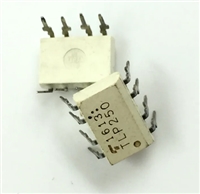
 TLP250光耦合器:资料手册参数分析

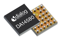
 DA14580 低功耗蓝牙系统级芯片(SoC):资料手册参数分析

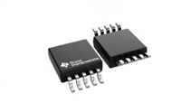
 INA226 高精度电流和功率监控器:资料手册参数分析

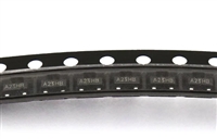
 SI2302 N沟道MOSFET:资料手册参数分析
