
 5秒后页面跳转

| 是否Rohs认证: | 不符合 | 生命周期: | Obsolete |
| Reach Compliance Code: | not_compliant | 风险等级: | 5.8 |
| JESD-30 代码: | R-PDIP-T24 | JESD-609代码: | e0 |
| 位数: | 8 | 端子数量: | 24 |
| 最高工作温度: | 85 °C | 最低工作温度: | -40 °C |
| 封装主体材料: | PLASTIC/EPOXY | 封装代码: | DIP |
| 封装等效代码: | DIP24,.6 | 封装形状: | RECTANGULAR |
| 封装形式: | IN-LINE | 电源: | 5/10 V |
| 子类别: | Parallel IO Port | 表面贴装: | NO |
| 技术: | CMOS | 温度等级: | INDUSTRIAL |
| 端子面层: | Tin/Lead (Sn/Pb) | 端子形式: | THROUGH-HOLE |
| 端子节距: | 2.54 mm | 端子位置: | DUAL |
| Base Number Matches: | 1 |
| 型号 | 品牌 | 获取价格 | 描述 | 数据表 |
| CDP1852C/3 | INTERSIL |
获取价格 |
High-Reliability Byte-Wide Input/Output Port |

|
| CDP1852CD | INTERSIL |
获取价格 |
Byte-Wide Input/Output Port |
|
| CDP1852CD/3 | RENESAS |
获取价格 |
IC 8 I/O, PIA-GENERAL PURPOSE, CDIP24, Parallel IO Port |
|
| CDP1852CD3 | INTERSIL |
获取价格 |
High-Reliability Byte-Wide Input/Output Port |
|
| CDP1852CDX | RENESAS |
获取价格 |
CDP1852CDX |
|
| CDP1852CE | INTERSIL |
获取价格 |
Byte-Wide Input/Output Port |
|
| CDP1852CEX | RENESAS |
获取价格 |
IC,I/O PORT,8-BIT,CMOS,DIP,24PIN,PLASTIC |
|
| CDP1852D | INTERSIL |
获取价格 |
Byte-Wide Input/Output Port |
|
| CDP1852D/3 | RENESAS |
获取价格 |
IC 8 I/O, PIA-GENERAL PURPOSE, CDIP24, Parallel IO Port |
|
| CDP1852D3 | INTERSIL |
获取价格 |
High-Reliability Byte-Wide Input/Output Port |
|
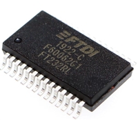 FT232RL资料解读:引脚说明、参数详情、产品特性

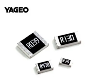
 RC0402FR-07100KL资料解读:电气参数、产品特性
 RC0603FR-070R数据手册解读:特性、应用与替换型号推荐
 ULC1001数据手册解读:产品特性、替换型号推荐
工作时间:9:00-21:00
CEO邮箱:ceo@jiepei.com
投诉邮箱:tousu@jiepei.com


 浙公网安备 33010502006866号 浙ICP备10014259号-119
营业执照ICP证
浙公网安备 33010502006866号 浙ICP备10014259号-119
营业执照ICP证


