ADSP-21065L
structures required in digital signal processing, and are com-
monly used in digital filters and Fourier transforms. The
ADSP-21065L’s two DAGs contain sufficient registers to allow
the creation of up to 32 circular buffers (16 primary register
sets, 16 secondary). The DAGs automatically handle address
pointer wraparound, reducing overhead, increasing perfor-
mance, and simplifying implementation. Circular buffers can
start and end at any memory location.
Off-Chip Memory and Peripherals Interface
The ADSP-21065L’s external port provides the processor’s
interface to off-chip memory and peripherals. The 64M words,
off-chip address space is included in the ADSP-21065L’s
unified address space. The separate on-chip buses—for program
memory, data memory and I/O—are multiplexed at the external
port to create an external system bus with a single 24-bit
address bus, four memory selects, and a single 32-bit data bus.
The on-chip Super Harvard Architecture provides three bus
performance, while the off-chip unified address space gives
flexibility to the designer.
Flexible Instruction Set
The 48-bit instruction word accommodates a variety of parallel
operations, for concise programming. For example, the ADSP-
21065L can conditionally execute a multiply, an add, a subtract
and a branch, all in a single instruction.
SDRAM Interface
The SDRAM interface enables the ADSP-21065L to transfer
data to and from synchronous DRAM (SDRAM) at 2x clock
frequency. The synchronous approach coupled with 2x clock
frequency supports data transfer at a high throughput—up to
220 Mbytes/sec.
ADSP-21065L FEATURES
The ADSP-21065L is designed to achieve the highest system
throughput to enable maximum system performance. It can be
clocked by either a crystal or a TTL-compatible clock signal.
The ADSP-21065L uses an input clock with a frequency equal
to half the instruction rate—a 33 MHz input clock yields a
15 ns processor cycle (which is equivalent to 66 MHz). Inter-
faces on the ADSP-21065L operate as shown below. Hereafter
in this document, 1x = input clock frequency, and 2x = processor’s
instruction rate.
The SDRAM interface provides a glueless interface with stan-
dard SDRAMs—16 Mb, 64 Mb, and 128 Mb—and includes
options to support additional buffers between the ADSP-21065L
and SDRAM. The SDRAM interface is extremely flexible and
provides capability for connecting SDRAMs to any one of the
ADSP-21065L’s four external memory banks.
Systems with several SDRAM devices connected in parallel may
require buffering to meet overall system timing requirements.
The ADSP-21065L supports pipelining of the address and
control signals to enable such buffering between itself and
multiple SDRAM devices.
The following clock operation ratings are based on 1x = 33 MHz
(instruction rate/core = 66 MHz):
SDRAM
External SRAM
Serial Ports
Multiprocessing
Host (Asynchronous)
66 MHz
33 MHz
33 MHz
33 MHz
33 MHz
Host Processor Interface
The ADSP-21065L’s host interface provides easy connection to
standard microprocessor buses—8-, 16-, and 32-bit—requiring
little additional hardware. Supporting asynchronous transfers at
speeds up to 1x clock frequency, the host interface is accessed
through the ADSP-21065L’s external port. Two channels of
DMA are available for the host interface; code and data trans-
fers are accomplished with low software overhead.
Augmenting the ADSP-21000 family core, the ADSP-21065L
adds the following architectural features:
Dual-Ported On-Chip Memory
The ADSP-21065L contains 544 Kbits of on-chip SRAM,
organized into two banks: Bank 0 has 288 Kbits, and Bank 1 has
256 Kbits. Bank 0 is configured with 9 columns of 2K ¥ 16 bits,
and Bank 1 is configured with 8 columns of 2K ¥ 16 bits. Each
memory block is dual-ported for single-cycle, independent accesses
by the core processor and I/O processor or DMA controller.
The dual-ported memory and separate on-chip buses allow two
data transfers from the core and one from I/O, all in a single
cycle (see Figure 4 for the ADSP-21065L Memory Map).
The host processor requests the ADSP-21065L’s external bus
with the host bus request (HBR), host bus grant (HBG), and
ready (REDY) signals. The host can directly read and write the
IOP registers of the ADSP-21065L and can access the DMA
channel setup and mailbox registers. Vector interrupt support
enables efficient execution of host commands.
DMA Controller
On the ADSP-21065L, the memory can be configured as a
maximum of 16K words of 32-bit data, 34K words for 16-bit
data, 10K words of 48-bit instructions (and 40-bit data) or
combinations of different word sizes up to 544 Kbits. All the
memory can be accessed as 16-bit, 32-bit or 48-bit.
The ADSP-21065L’s on-chip DMA controller allows zero-
overhead, nonintrusive data transfers without processor inter-
vention. The DMA controller operates independently and
invisibly to the processor core, allowing DMA operations to
occur while the core is simultaneously executing its program
instructions.
While each memory block can store combinations of code and
data, accesses are most efficient when one block stores data,
using the DM bus for transfers, and the other block stores
instructions and data, using the PM bus for transfers. Using the
DM and PM busses in this way, with one dedicated to each
memory block, assures single-cycle execution with two data
transfers. In this case, the instruction must be available in the
cache. Single-cycle execution is also maintained when one of
the data operands is transferred to or from off-chip, via the
ADSP-21065L’s external port.
DMA transfers can occur between the ADSP-21065L’s internal
memory and either external memory, external peripherals, or a
host processor. DMA transfers can also occur between the
ADSP-21065L’s internal memory and its serial ports. DMA
transfers between external memory and external peripheral
devices are another option. External bus packing to 16-, 32-, or
48-bit internal words is performed during DMA transfers.
Ten channels of DMA are available on the ADSP-21065L—
eight via the serial ports, and two via the processor’s external
port (for either host processor, other ADSP-21065L, memory or
–4–
REV. C


 SI2301 N沟道MOSFET:资料手册参数分析

 ADC0809逐次逼近寄存器型模数转换器:资料手册参数分析

 AD9361捷变收发器:全面参数解析与关键特性概览

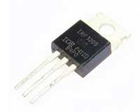
 IRF3205功率MOSFET:资料手册参数分析
