
 5秒后页面跳转

| 型号 | 品牌 | 获取价格 | 描述 | 数据表 |
| ADAQ7768-1 | ADI |
获取价格 |
24位单通道精密μModule数据采集系统 |

|
| ADAQ7769-1 | ADI |
获取价格 |
High Input Impedance, Programmable Gain, 24-B |
|
| ADAQ7980 | ADI |
获取价格 |
16-Bit, 1 MSPS, Integrated Data Acquisition Subsystem |
|
| ADAQ7980BCCZ | ADI |
获取价格 |
16-Bit, 1 MSPS, Integrated Data Acquisition Subsystem |
|
| ADAQ7980BCCZ-RL7 | ADI |
获取价格 |
16-Bit, 1 MSPS, Integrated Data Acquisition Subsystem |
|
| ADAQ7988 | ADI |
获取价格 |
16-Bit, 1 MSPS, Integrated Data Acquisition Subsystem |
|
| ADAQ7988BCCZ | ADI |
获取价格 |
16-Bit, 1 MSPS, Integrated Data Acquisition Subsystem |
|
| ADAQ7988BCCZ-RL7 | ADI |
获取价格 |
16-Bit, 1 MSPS, Integrated Data Acquisition Subsystem |
|
| ADAQ8088 | ADI |
获取价格 |
具有增益和 ADC 驱动器的双路、差分、低通滤波器 μModule |
|
| ADAQ8092 | ADI |
获取价格 |
14位、105 MSPSμ模块 |
|
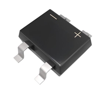 数据手册解读:MB10S引脚说明、电气参数

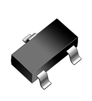 2N7002K资料解读:产品特性和型号推荐
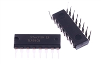 资料解读:TL494CN参数和引脚功能图说明
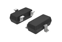 解读BAT54A数据手册:全面解析产品特性与应用
工作时间:9:00-21:00
CEO邮箱:ceo@jiepei.com
投诉邮箱:tousu@jiepei.com


 浙公网安备 33010502006866号 浙ICP备10014259号-119
营业执照ICP证
浙公网安备 33010502006866号 浙ICP备10014259号-119
营业执照ICP证


